Semiconductor device comprising buried wiring layer

a technology of buried wiring layer and semiconductor device, which is applied in the direction of radiation control device, transistor, basic electric element, etc., can solve the problems of limited miniaturization of ldmosfet, reducing the area occupied, and the need for power transistor miniaturization

Active Publication Date: 2010-01-12
SEMICON COMPONENTS IND LLC
View PDF38 Cites 9 Cited by
  • Summary
  • Abstract
  • Description
  • Claims
  • Application Information

AI Technical Summary

Benefits of technology

[0008]The present invention provides a semiconductor device and a method for manufacturing a semiconductor device that prevents local concentration of current from causing partial discharging to a semiconductor substrate.

Problems solved by technology

This has resulted in a requirement for miniaturization of power transistors used in such electronic devices.
However, the miniaturization of the LDMOSFET is limited by the existence of the drift region.
However, reduction in the area occupied by each semiconductor element reduces regions for formation of metal wires that connect semiconductor elements or connect each semiconductor element to an external circuit.
This reduces the wiring width of the metal wires and increases the wiring resistance of the metal wires, which lead to the problems described below.
The current concentration may lower the reliability of the semiconductor elements or shorten the lifetime of the wires with respect to fusion and electronic migration.
Although the DMOSFET is less likely to have a secondary breakdown than a bipolar transistor, local concentration of current may inflict damages to a DMOSFET.

Method used


Image

  • Semiconductor device comprising buried wiring layer
  • Semiconductor device comprising buried wiring layer
  • Semiconductor device comprising buried wiring layer

Examples


first embodiment

[0046]A semiconductor device according to the present invention will now be described with reference to the drawings.

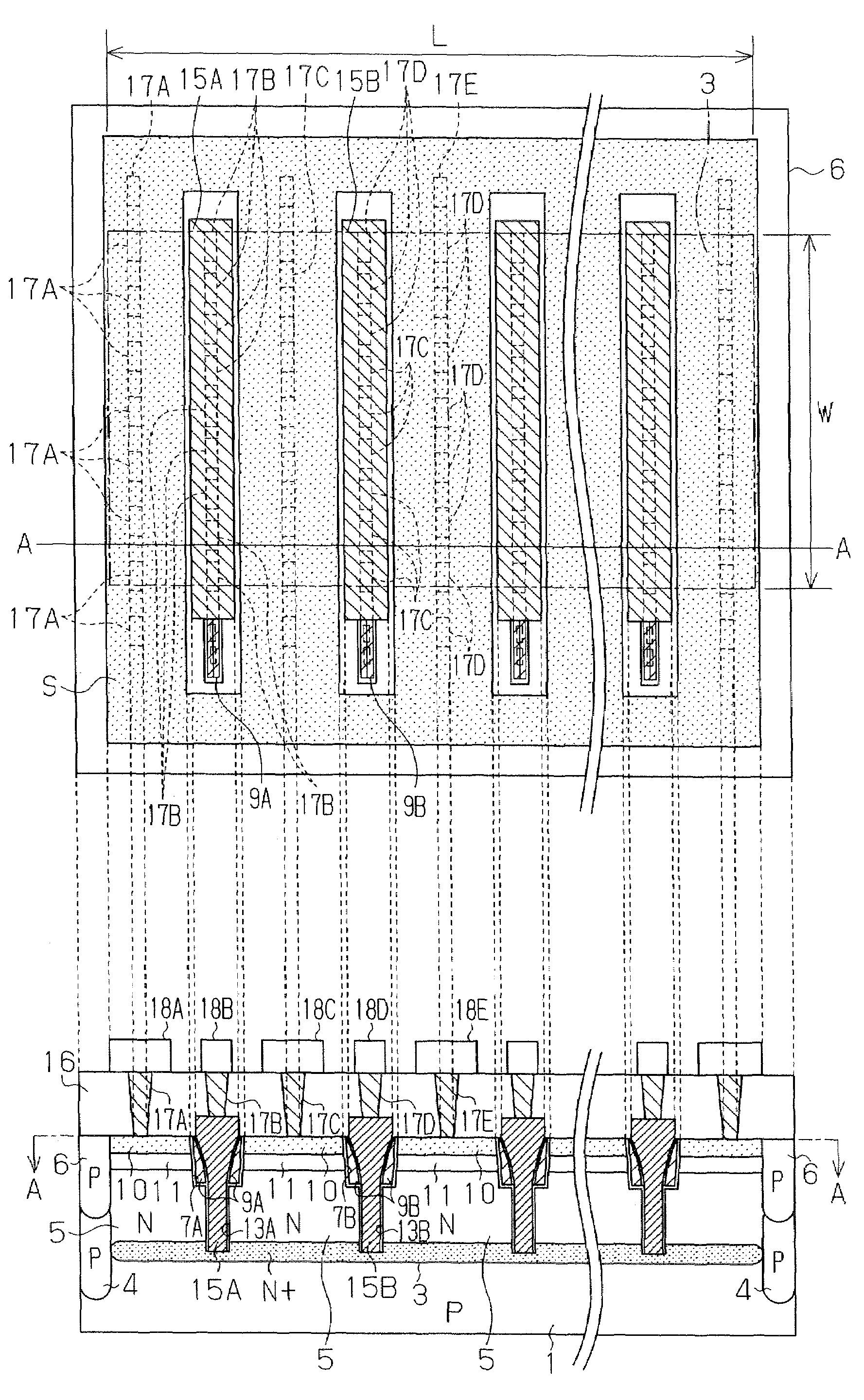
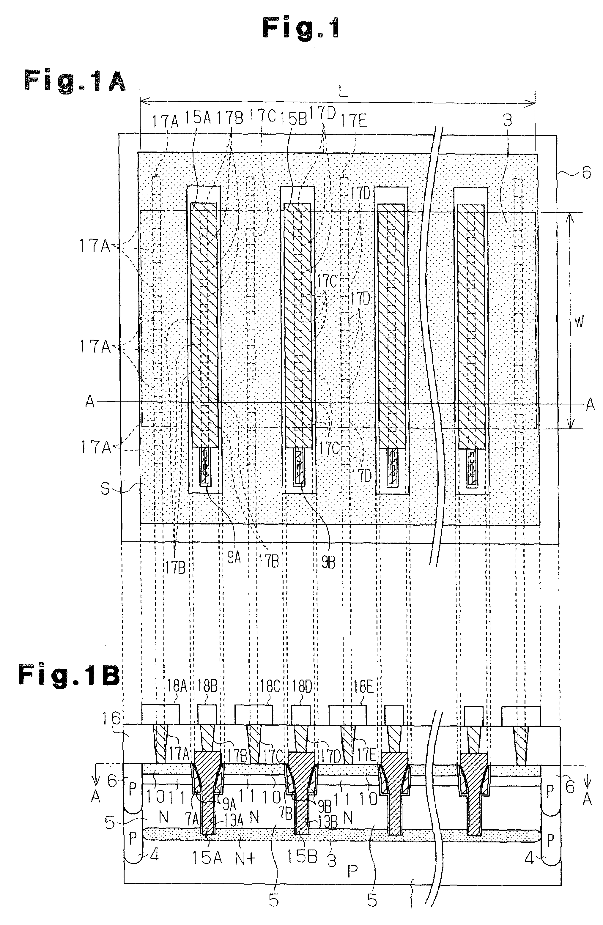
[0047]The structure of the semiconductor device according to the first embodiment will now be described in detail with reference to FIGS. 1A and 1B. FIG. 1A is a plane view showing the semiconductor device, and FIG. 1B is a cross-sectional view taken along line A-A in FIG. 1A.

[0048]As shown in FIG. 1A, the semiconductor device of the first embodiment includes a plurality of double diffused metal oxide semiconductor field effect transistors (hereafter referred to as “DMOSFETs”) arranged in a semiconductor element formation region S surrounded by isolation diffusion layers 4 and 6. The semiconductor device may be used for example as a power transistor. The problem of the DMOSFET, which typically has a total gate length of as long as several millimeters, is in that it has a high wiring resistance. To solve this problem, the DMOSFETs are arranged to form a multi-finger st...

second embodiment

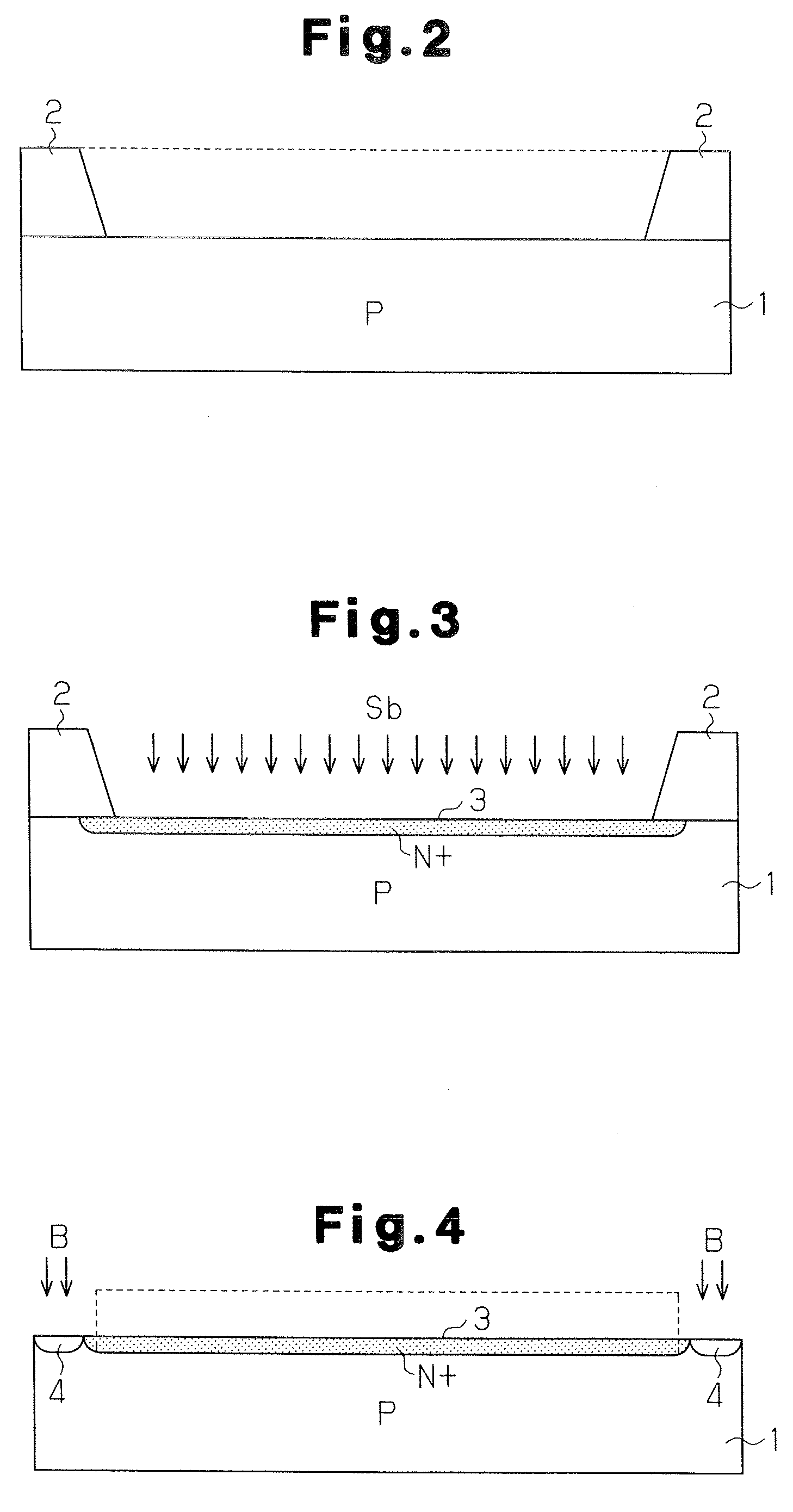
[0083]An n-type silicon epitaxial layer 33 is formed on a p-type monocrystalline silicon substrate 32. A p-type isolation diffusion layer 35 extends through the substrate 32 and the epitaxial layer 33 so as to form an island region. Although FIG. 14 shows only one island region in the second embodiment, a plurality of island regions are actually formed. A vertical transistor, such as an N-channel MOS transistor, a P-channel MOS transistor, or an NPN transistor, may be formed in each island region.

[0084]An n-type buried layer 38 is formed between the substrate 32 and the epitaxial layer 33 with the interface of the substrate 32 and the epitaxial layer 33 located therein. The buried layer 38 is formed within the range of a semiconductor element formation region that is formed above the buried layer 38. Inner side walls of a first trench 39 are covered by a silicon oxide film 41 for insulating the drain and the substrate. A portion of the silicon oxide film 41 is removed from the botto...


PUM


Abstract

A semiconductor device that suppresses partial discharging to a semiconductor substrate caused by local concentration of current. The semiconductor device includes a semiconductor substrate, a gate electrode buried in the semiconductor substrate, a conductor buried in the semiconductor substrate further inward from the gate electrode, a wiring layer formed in the semiconductor substrate in connection with the conductor, and an insulation film arranged between the gate electrode and the conductor. The conductor is higher than the surface of the semiconductor substrate.

Description

CROSS-REFERENCE TO RELATED APPLICATIONS[0001]This application is based upon and claims the benefit of priority from the prior Japanese Patent Applications No. 2006-179119, filed on Jun. 29, 2006, and No. 2007-141961, filed on May 29, 2007, the entire contents of which are incorporated herein by reference.BACKGROUND OF THE INVENTION[0002]The present invention relates to a semiconductor device, and more particularly, to a semiconductor device, which includes a plurality of power transistors, that has a structure enabling miniaturization and improves operational stability.[0003]The size and cost of electronic devices have been reduced. This has resulted in a requirement for miniaturization of power transistors used in such electronic devices. In particular, electronic devices that operate at withstand voltages of 100 V and lower, such as portable devices and household appliances, are required to be further miniaturized. Such electronic devices must employ a technique for integrating a ...

Claims


Application Information

Patent Timeline
Patent Type & Authority Patents(United States)
IPC IPC(8): H01L27/01H01L23/48H01L23/52H01L27/10H01L27/12H01L27/148H01L29/40H01L29/73H01L29/74H01L29/749H01L29/76H01L29/768H01L29/94H01L31/062H01L31/113H01L31/119H01L21/3205H01L21/336H01L21/768H01L23/522H01L29/41H01L29/423H01L29/49H01L29/78
CPCH01L29/66553H01L29/66621H01L29/7816H01L21/28114H01L29/42376H01L29/4238H01L21/743
Inventor YAMAOKA, YOSHIKAZUSHIMADA, SATORU
Owner SEMICON COMPONENTS IND LLC
Why Eureka
Try Eureka