Organic light emitting element

a light-emitting element and organic technology, applied in the direction of thermoelectric device junction materials, electrical equipment, semiconductor devices, etc., can solve the problems of difficult to obtain features and short lifetimes, and achieve the effect of longer lifetimes

Active Publication Date: 2010-01-19
SEMICON ENERGY LAB CO LTD
View PDF42 Cites 26 Cited by
  • Summary
  • Abstract
  • Description
  • Claims
  • Application Information

AI Technical Summary

Benefits of technology

[0029]In a light-emitting element of the present invention, a light-emitting region is formed in the vicinity of the center of a light-emitting layer, instead of at the interface between the light-emitting layer and a hole-transporting layer or at the interface between the light-emitting layer and an electron-transporting layer, and thus, the light-emitting element deteriorates less due to the light-emitting region adjacent to the hole-transporting layer or the electron-transporting layer. In other words, the change with time of luminance is small and a light-emitting element having a long lifetime can be provided.
[0030]Further, a light-emitting element of the present invention is applied to light-emitting devices and electronic devices, so that the light-emitting devices and the electronic devices can have longer lifetimes.

Problems solved by technology

This is a feature which is difficult to be obtained by point light sources typified by an incandescent lamp and an LED or linear light sources typified by a fluorescent lamp.
Such a light-emitting element including a light-emitting organic compound can be driven at lower voltage than a light-emitting element using an inorganic compound; however, such a light-emitting element including a light-emitting organic compound has a problem in that its lifetime is short.

Method used


Image

  • Organic light emitting element
  • Organic light emitting element
  • Organic light emitting element

Examples


embodiment mode 1

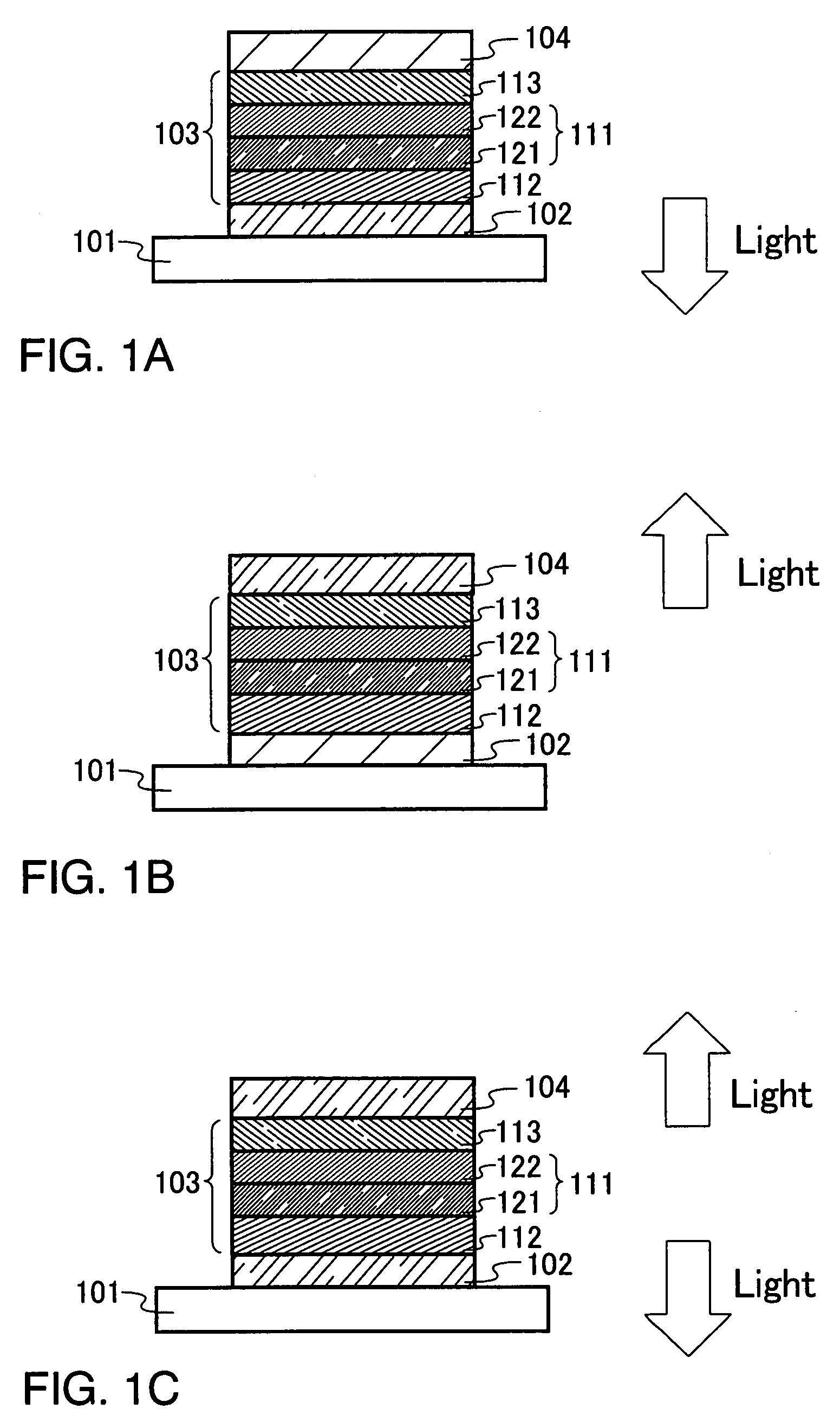
[0066]One mode of a light-emitting element of the present invention will be described hereinafter with reference to FIG. 1A.

[0067]The light-emitting element of the present invention includes a plurality of layers between a pair of electrodes. In this specification, the plurality of layers formed between the pair of electrodes is collectively referred to as an EL layer.

[0068]In this embodiment mode, the light-emitting element includes a first electrode 102, a second electrode 104 and an EL layer 103 formed between the first electrode 102 and the second electrode 104. In addition, in this embodiment mode, the first electrode 102 serves as an anode and the second electrode 104 serves as a cathode. In other words, when a voltage is applied to the first electrode 102 and the second electrode 104 such that a potential of the first electrode 102 is higher than that of the second electrode 104, light emission can be obtained. Such a case will be described below.

[0069]The substrate 101 is us...

embodiment mode 2

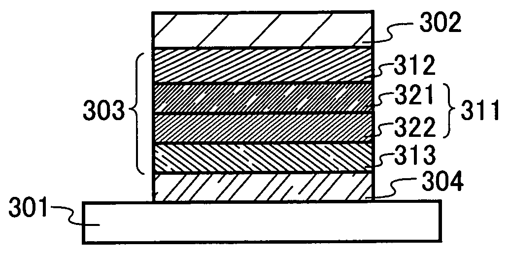
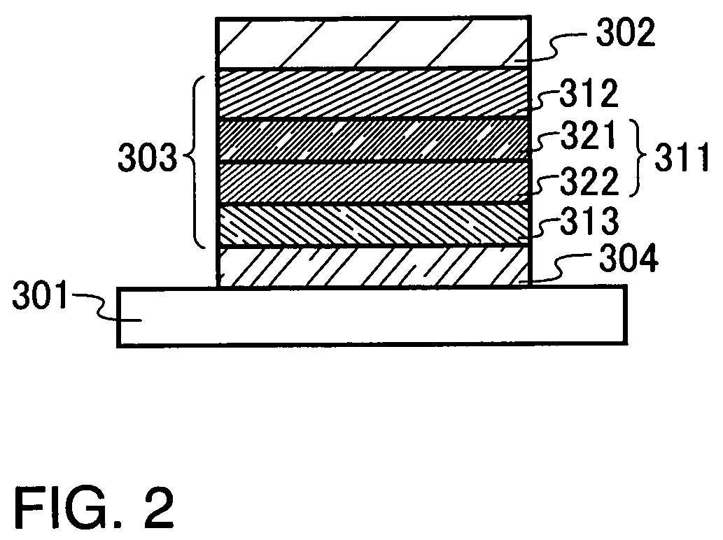
[0110]Embodiment Mode 2 will describe a mode of a light-emitting element in which a plurality of light-emitting units in accordance with the present invention are stacked (hereinafter, also referred to as a stacked type light-emitting element) with reference to FIG. 3. This light-emitting element is a light-emitting element including a plurality of light-emitting units between a first electrode and a second electrode. As the light-emitting units, a structure similar to that of the EL layer shown in Embodiment Mode 1 can be used, In other words, the light-emitting element shown in Embodiment Mode 1 is a light-emitting element having one light-emitting unit, and Embodiment Mode 2 will describe a light-emitting element having a plurality of light-emitting units.

[0111]In FIG. 3, a first light-emitting unit 511 and a second light-emitting unit 512 are stacked between a first electrode 501 and a second electrode 502. To the first electrode 501 and the second electrode 502, similar electro...

embodiment mode 3

[0118]Embodiment Mode 3 will describe a light-emitting device having a light-emitting element of the present invention.

[0119]This embodiment mode will describe a light-emitting device having a light-emitting element of the present invention in a pixel portion, with reference to FIGS. 4A and 4B. FIG. 4A is a top view illustrating a light-emitting device while FIG. 4B is a cross-sectional view along lines A-A′ and B-B′ of FIG. 4A. A reference numeral 601 shown with a dotted line denotes a driver circuit portion (source side driver circuit); 602, a pixel portion; and 603, a driver circuit portion (gate side driver circuit). Moreover, a reference numeral 604 denotes a sealing substrate; 605, a sealing material; and 607, a space surrounded by the sealing material 605.

[0120]A leading wire 608 is to transmit a signal to be inputted to the source side driver circuit 601 and the gate side driver circuit 603, and receive a video signal, a clock signal, a start signal, a reset signal, and the ...


PUM


Abstract

The present invention provides a light-emitting element including an electron-transporting layer and a hole-transporting layer between a first electrode and a second electrode; and a first layer and a second layer between the electron-transporting layer and the hole-transporting layer, wherein the first layer includes a first organic compound and an organic compound having a hole-transporting property, the second layer includes a second organic compound and an organic compound having an electron-transporting property, the first layer is formed in contact with the first electrode side of the second layer, the first organic compound and the second organic compound are the same compound, and a voltage is applied to the first electrode and the second electrode, so that both of the first organic compound and the second organic compound emit light.

Description

TECHNICAL FIELD[0001]The present invention relates to current excitation type light-emitting elements. Further, the present invention relates to light-emitting devices and electronic devices having the light-emitting element.BACKGROUND OF THE INVENTION[0002]In recent years, research and development have been extensively conducted on light-emitting elements using electroluminescence. In a basic structure of such a light-emitting element, a substance having a light-emitting property is interposed between a pair of electrodes. By voltage application to this element, light emission can be obtained from the substance having a light-emitting property.[0003]Since such a light-emitting element is of self-light-emitting type, it is considered that the light-emitting element has advantages over a liquid crystal display in that visibility of pixels is high, backlight is not required, and so on and is therefore suitable as flat panel display elements. In addition, other advantages of such a lig...

Claims


Application Information

Patent Timeline
Patent Type & Authority Patents(United States)
IPC IPC(8): H01L29/24H01L27/14H01L29/08H01L31/00H01L31/0232H01L33/00H01L35/24H01L51/00
CPCH01L51/5012H01L51/5072H01L51/5056H01L51/5048H10K50/14H10K50/11H10K50/15H10K50/16H10K85/615
Inventor OHSAWA, NOBUHARU
Owner SEMICON ENERGY LAB CO LTD
Why Eureka
Try Eureka