Semiconductor device and a manufacturing method of the same

a semiconductor device and manufacturing method technology, applied in the field of semiconductor devices, can solve the problems of inability to meet the required board size and wire length, and achieve the effect of reducing the size of the semiconductor device and improving the manufacturing yield of the semiconductor devi

Active Publication Date: 2010-02-02
RENESAS ELECTRONICS CORP
View PDF7 Cites 10 Cited by
  • Summary
  • Abstract
  • Description
  • Claims
  • Application Information

AI Technical Summary

Benefits of technology

[0014]For reducing the size of the BGA type semiconductor device it is necessary to reduce the planar size of a wiring board. For reducing the planar size of a wiring board it is necessary to narrow the layout pitch of electrode pads on the wiring board and shorten the length of a pad row consisting of plural electrode pads.
[0037]According to the present invention it is possible to improve the semiconductor device manufacturing yield.

Problems solved by technology

In such a single-row layout of pads, however, it is impossible to satisfy required board size and wire length.

Method used


Image

  • Semiconductor device and a manufacturing method of the same
  • Semiconductor device and a manufacturing method of the same
  • Semiconductor device and a manufacturing method of the same

Examples


first embodiment

[0060]In this first embodiment a description will be given below about an example of application of the present invention to an SIP (System In Package) type semiconductor device wherein plural semiconductor chips with integrated circuits of different functions formed thereon are mounted on a wiring substrate to build a single system.

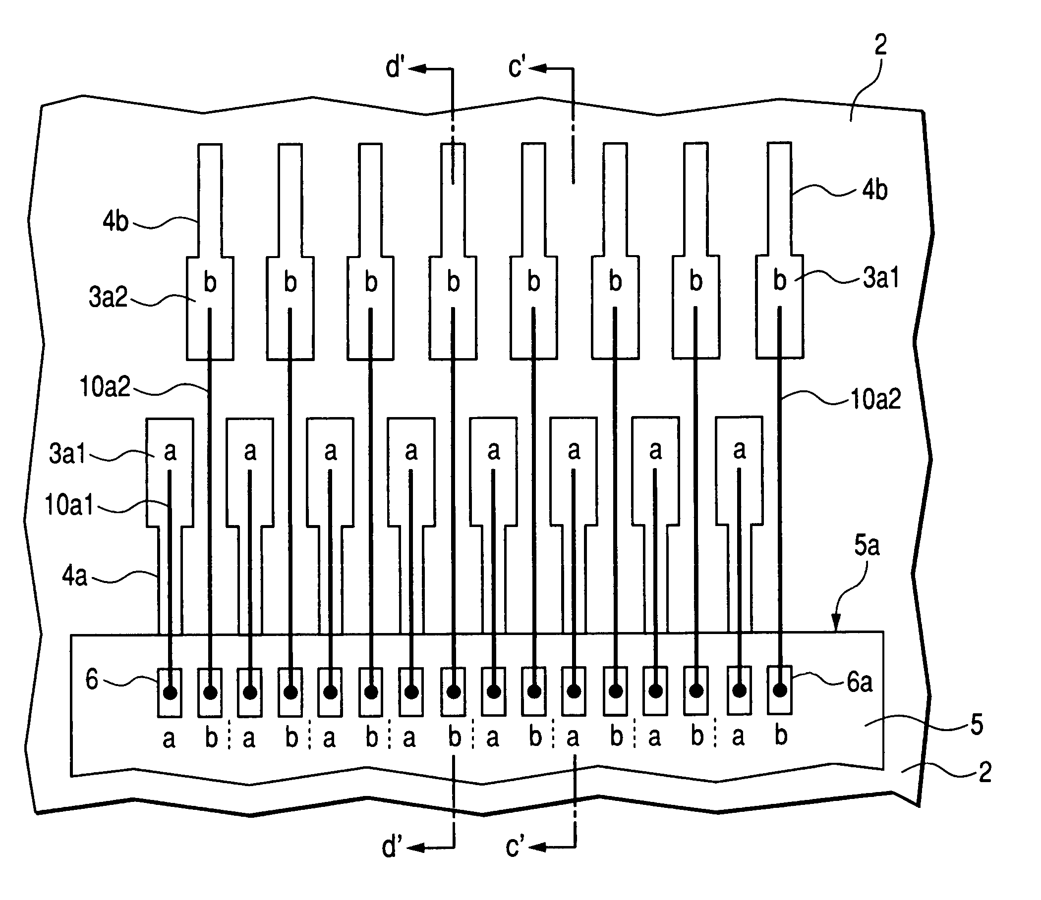
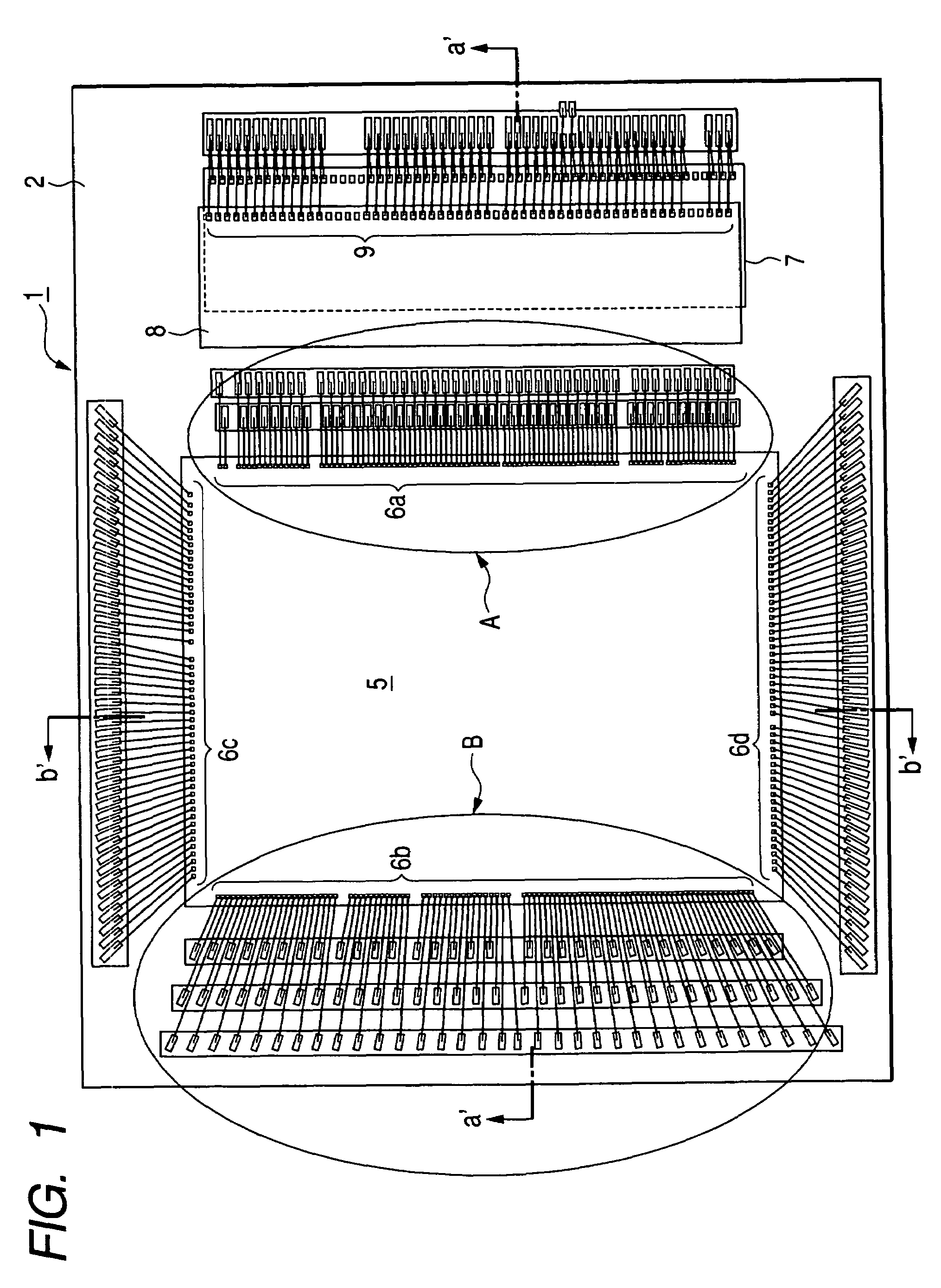
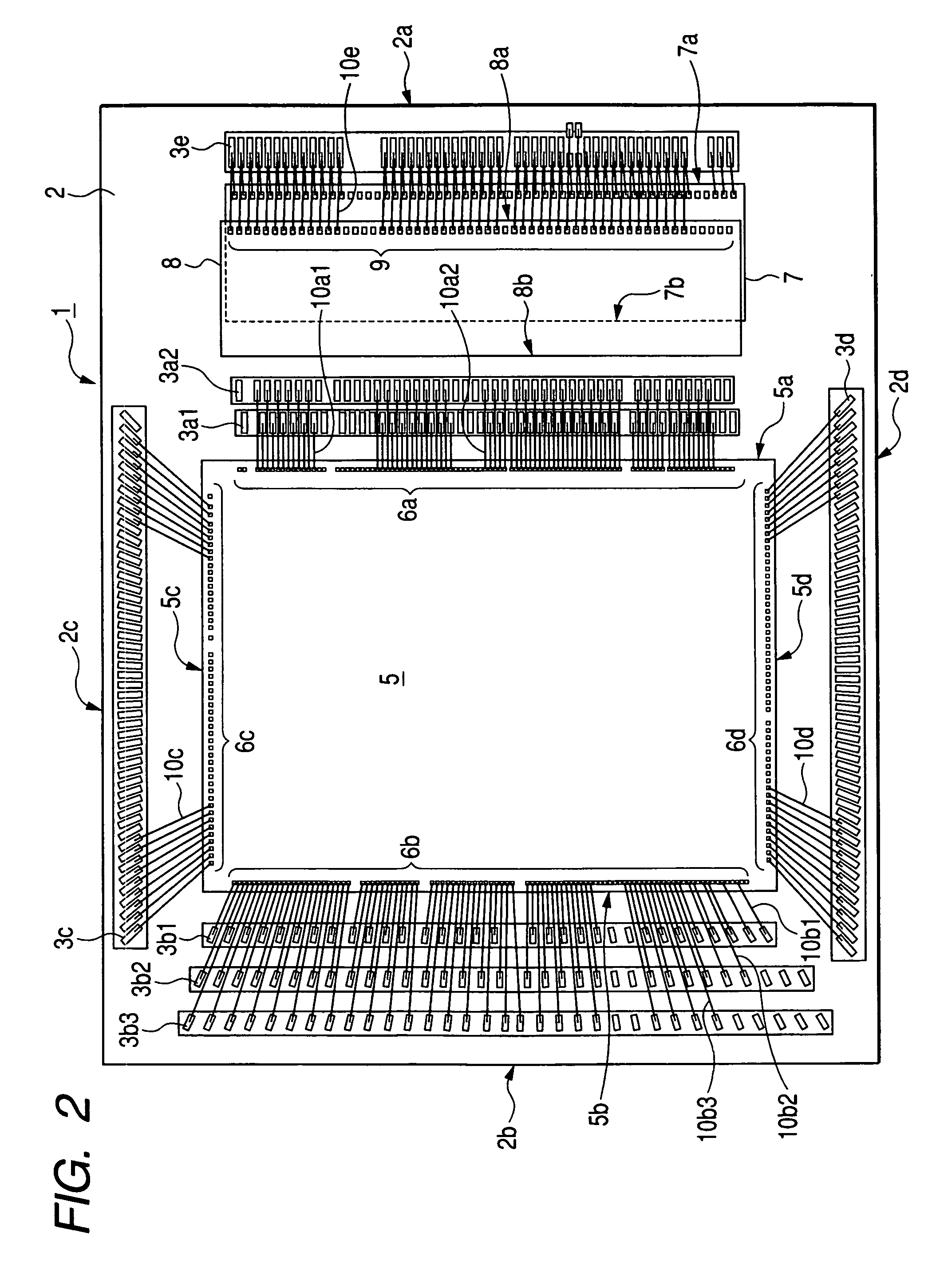
[0061]FIGS. 1 to 16 illustrate a semiconductor device according to a first embodiment of the present invention, of which FIG. 1 is a schematic plan view showing an internal structure of the semiconductor device, FIG. 2 is a schematic plan view showing a partially omitted state of bonding wires in FIG. 1, FIG. 3 is a schematic sectional view taken on line a′-a′ in FIG. 1, FIG. 4 is a schematic sectional view taken on line b′-b′ in FIG. 1, FIG. 5 is a schematic plan view showing a part (portion A) of FIG. 1 in a simplified manner, FIG. 6 is a schematic plan view showing an omitted state of bonding wires in FIG. 5, FIG. 7 is a schematic sectional view taken...

second embodiment

[0133]FIG. 17 is a schematic plan view showing a schematic construction of a semiconductor device according to a second embodiment of the present invention and FIG. 18 is a schematic plan view showing an omitted state of bonding wires in FIG. 17.

[0134]This second embodiment is an example in which the present invention for diminishing the layout pitch of pads is applied to a three-row pads layout.

[0135]As shown in FIGS. 17 and 18, electrode pads 3a1 (a) confront corresponding electrode pads 6a (a), electrode pads 3a2 (b) confront corresponding electrode pads 6a (b), and electrode pads 3a3 (c) confront corresponding electrode pads 6a (c).

[0136]The layout pitch n1 of electrode pads 3a1 (a), the layout pitch n2 of electrode pads 3a2 (b), and the layout pitch n3 of electrode pads 3a3 (c), are three times as large as the layout pitch m1 of electrode pads 6a of the semiconductor chip 5 in terms of design values.

[0137]The layout pitch n12 between the electrode pads 3a1 (a), 3a2 (b) and the ...

third embodiment

[0140]FIG. 19 is a schematic diagram showing a schematic construction of a semiconductor device according to a third embodiment of the present invention and FIG. 20 is a schematic plan view showing an omitted state of bonding wires in FIG. 19.

[0141]This third embodiment is an example in which the present invention for diminishing the layout pitch of pads is applied to a four-row pads layout.

[0142]As shown in FIGS. 19 and 20, electrode pads 3a1 to 3a4 (a to d) confront corresponding electrode pads 6a (a to d). The layout pitch n1 of electrode pads 3a1 (a), the layout pitch n2 of electrode pads 3a2 (b), the layout pitch n3 of electrode pads 3a3 (c), and the layout pitch n4 of electrode pads 3a4 (d), are four times as large as the layout pitch m1 of electrode pads 6a.

[0143]The layout pitch n12 between the electrode pads 3a1, 3a2, the layout pitch n23 between the electrode pads 3a2, 3a3, and the layout pitch n34 between the electrode pads 3a3, 3a4, are the same as the layout pitch m1 o...


PUM


Abstract

A semiconductor device is disclosed wherein first wiring lines in a first row extend respectively from first connecting portions toward one side of a semiconductor chip, while second wiring lines extend respectively from second connecting portions toward the side opposite to the one side of the semiconductor chip. The reduction in size of the semiconductor device can be attained.

Description

CROSS-REFERENCE TO RELATED APPLICATION[0001]The present application claims priority from Japanese patent application No. 2005-287775 filed on Sep. 30, 2005, the content of which is hereby incorporated by reference into this application.BACKGROUND OF THE INVENTION[0002]The present invention relates a semiconductor device and a manufacturing technique for the same. Particularly, the present invention is concerned with a technique applicable effectively to a semiconductor device wherein electrode pads of a semiconductor chip and electrode pads of a wiring board are connected together through bonding wires.[0003]As a semiconductor device there is known, for example, a semiconductor device called BGA (Ball Grid Array) type. The BGA type semiconductor device is of a package structure wherein a semiconductor chip is mounted on a main surface side of a wiring board called interposer and plural ball-like solder bumps as external connecting terminals are arranged on a back surface side opposi...

Claims


Application Information

Patent Timeline
Patent Type & Authority Patents(United States)
IPC IPC(8): H01L23/495
CPCH01L23/49838H01L24/49H01L25/0652H01L2924/12041H01L24/45H01L24/85H01L2223/54486H01L2224/05553H01L2224/45144H01L2224/4809H01L2224/48091H01L2224/48095H01L2224/48227H01L2224/48228H01L2224/48465H01L2224/49171H01L2224/49175H01L2224/49431H01L2224/49433H01L2225/0651H01L2225/06562H01L2924/01002H01L2924/01004H01L2924/01005H01L2924/01007H01L2924/01013H01L2924/01014H01L2924/01029H01L2924/01078H01L2924/01079H01L2924/14H01L2924/15311H01L23/544H01L2224/48599H01L2224/32145H01L2224/73265H01L2224/32225H01L2224/48233H01L2224/85H01L2924/014H01L2924/01033H01L2924/01006H01L24/48H01L2924/00014H01L2924/00H01L2924/00012H01L2924/181H01L24/73H01L2224/05554H01L2924/15183
Inventor TSUTSUMI, YASUMIMIWA, TAKASHI
Owner RENESAS ELECTRONICS CORP
Why Eureka
Try Eureka