
Statistical optimization and design method for analog and digital circuits

a technology of statistic optimization and design method, applied in stochastic cad, cad techniques, instruments, etc., can solve the problems of increasing the difficulty of understanding the design, affecting the performance of analog/rf circuits, and complicated analog/rf circuit design, etc., to achieve high accuracy response surface, reduce computational costs, and improve computational efficiency

Active Publication Date: 2010-02-23
XIGMIX
View PDF4 Cites 14 Cited by
  • Summary
  • Abstract
  • Description
  • Claims
  • Application Information

AI Technical Summary

Benefits of technology

[0019]Many benefits are achieved by way of the present invention over conventional techniques. For example, embodiments of the present invention provide high accuracy response surface (e.g. polynomial and posynomial) models at low computational costs. Additionally, some embodiments of the present invention provide methods of performing statistical analysis using close-form models without the use of Monte Carlo techniques. As will be evident to one of skill in the art, the use of close-form models is generally more computationally efficient than the Monte Carlo techniques. Moreover, convex optimization processes using fitted performance models are provided by embodiments of the present invention, resulting in an increased probability of producing optimized circuit designs at the global minimum. Depending upon the embodiment, one or more of these benefits, as well as other benefits, may be achieved. These and other benefits will be described in more detail throughout the present specification and more particularly below in conjunction with the following drawings.

Problems solved by technology

For example, non-ideal effects such as parasitic coupling and process variations may adversely impact circuit performance.
As a result, in some cases, to account for these non-ideal effects, the analog / RF circuit design becomes more complicated, increasing the difficulty of understanding the design as well as increasing the difficulty of the design process.
Accordingly, manual design of present analog / RF circuits is generally a time-consuming process that requires a significant measure of design experience.
These stochastic search algorithms are generally extremely slow and result in expensive computation costs.
As will be evident to one of skill in the art, linear polynomial response surface models may not be sufficiently accurate and quadratic polynomial response surface models may produce non-optimal solutions when local minimums are present.
In addition, building the conventional quadratic models generally requires a great number of sampling points and solves a great number of unknown coefficients, yielding an extremely expensive computation cost.
A drawback of such manually derived equations is that this manual process applies various simplifications and may ignore many second-order effects.
However, these conventional methods are computationally expensive.
Building conventional quadratic response surface models, both polynomial and posynomial models, requires simulation at a large number of sampling points, resulting in expensive computation costs.
Moreover, building these conventional quadratic response surface models entails the solution of a large number of unknown coefficients, also resulting in expensive computation costs.
As a result of these drawbacks, conventional response surface modeling approaches are generally only applicable to small and medium size circuit designs.
The inclusion of these process variations generally results in an additional increase in the computation cost necessary to determine an optimal solution.
Often, the equation-based optimization processes use simplified equations that can introduce error into the search results.
As discussed above, this step is typically a simulation-based optimization that is either oversimplified to produce a tractable problem or prohibitively expensive in computational terms.

Method used


Image

  • Statistical optimization and design method for analog and digital circuits
  • Statistical optimization and design method for analog and digital circuits
  • Statistical optimization and design method for analog and digital circuits

Examples


Embodiment Construction

[0030]According to the present invention techniques related to integrated circuit modeling and optimization are provided. More specifically, the present invention relates to the design of analog / RF and digital circuits based on device level simulation models incorporating process and environmental variations. Merely by way of example, the invention has been applied to statistical analysis and optimization of analog / RF and digital circuits. The methods and techniques can be applied to other applications as well such as MEMS design, radiation hardened circuit design, statistical process control, and the like.

[0031]Embodiments of the present invention provide analog / RF design tools that incorporate the impact of process and environmental variations. As device dimensions decrease, for example with sub-100 nm technologies, consideration of the process and environmental variations becomes a critical design concern. Using conventional design techniques lacking the inclusion of process and ...


PUM


Abstract

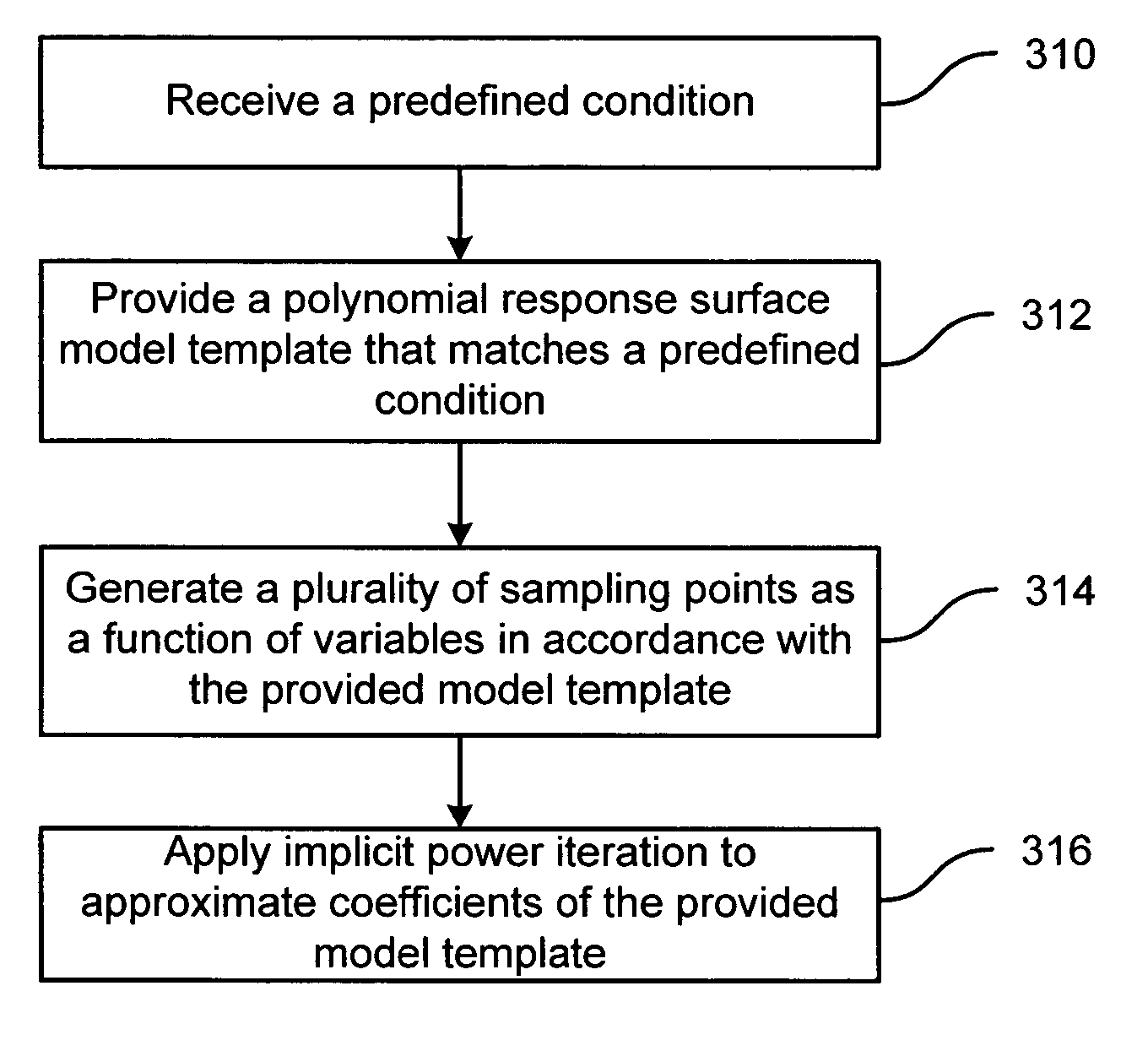
A computer implemented method of performing projection based polynomial fitting. The method includes generating a plurality of sampling points as a function of variables. The method also includes forming a polynomial model template representative of the plurality of sampling points. According to embodiments of the present invention, the polynomial model template comprises at least one polynomial coefficient. The method further includes forming a low-rank matrix to approximate the polynomial coefficient.

Description

CROSS-REFERENCES TO RELATED APPLICATIONS[0001]This application claims priority to U.S. Provisional Application Ser. No. 60 / 623,176, filed Oct. 29, 2004, entitled “Robust Analog / RF Design with Projection-Based Performance Modeling,” the disclosure of which is incorporated herein by reference in its entirety.BACKGROUND OF THE INVENTION[0002]The present invention relates generally to integrated circuit modeling and optimization techniques. More specifically, the present invention relates to the design of analog / RF and digital circuits based on device level simulation models incorporating process and environmental variations. Merely by way of example, the invention has been applied to statistical analysis and optimization of analog / RF and digital circuits. The methods and techniques can be applied to other applications as well such as MEMS design, radiation hardened circuit design, statistical process control, and the like.[0003]As IC technologies are scaled to finer feature sizes (e.g....

Claims


Application Information

Patent Timeline
Patent Type & Authority Patents(United States)
IPC IPC(8): G06F17/50G06F9/45
CPCG06F17/5036G06F2217/10G06F30/367G06F2111/08
Inventor LI, XINPILEGGI, LARRY
Owner XIGMIX
Learn More