Fabrication of semiconductor device having composite contact

a technology of semiconductor devices and contact surfaces, applied in the direction of semiconductor devices, basic electric elements, electrical equipment, etc., can solve the problems of reducing limiting the performance of the device, and so as to achieve the effect of reducing the contact resistan

Active Publication Date: 2010-03-09
SENSOR ELECTRONICS TECH
View PDF16 Cites 10 Cited by
  • Summary
  • Abstract
  • Description
  • Claims
  • Application Information

AI Technical Summary

Benefits of technology

[0007]Aspects of the invention provide a method of fabricating a semiconductor device with a composite contact. The fabrication includes forming the composite contact to a semiconductor layer in a semiconductor structure. The composite contact is formed by forming a direct current (DC) conducting electrode attached to a semiconductor layer in a semiconductor structure and forming a capacitive electrode that is partially over the DC conducting electrode and extends beyond the DC conducting electrode. The composite contact provides a combined resistive-capacitive coupling to the semiconductor layer. As a result, a contact impedance is reduced when the corresponding semiconductor device is operated at high frequencies.

Problems solved by technology

For example, contact resistance significantly affects the performance characteristics of the semiconductor device.
However, in many high-frequency semiconductor devices, the resistance of the contact is a dominant factor in limiting the performance of the device.
Such annealing remains a challenging technology, especially for wide bandgap semiconductor materials.
Additionally, contact formation becomes even more challenging with novel emerging wide bandgap material systems and devices, such as material systems / devices based on aluminum nitride (AlN), diamond, and others.
While advanced annealing techniques have been shown to yield lower unit-width contact resistances, the general trend in which high annealing temperatures lead to significant morphology degradation, defect generation, and contact edge roughness remains.
Further, the under annealed contact does not provide any ability to achieve self-aligned or alignment-free fabrication.

Method used


Image

  • Fabrication of semiconductor device having composite contact
  • Fabrication of semiconductor device having composite contact
  • Fabrication of semiconductor device having composite contact

Examples


Embodiment Construction

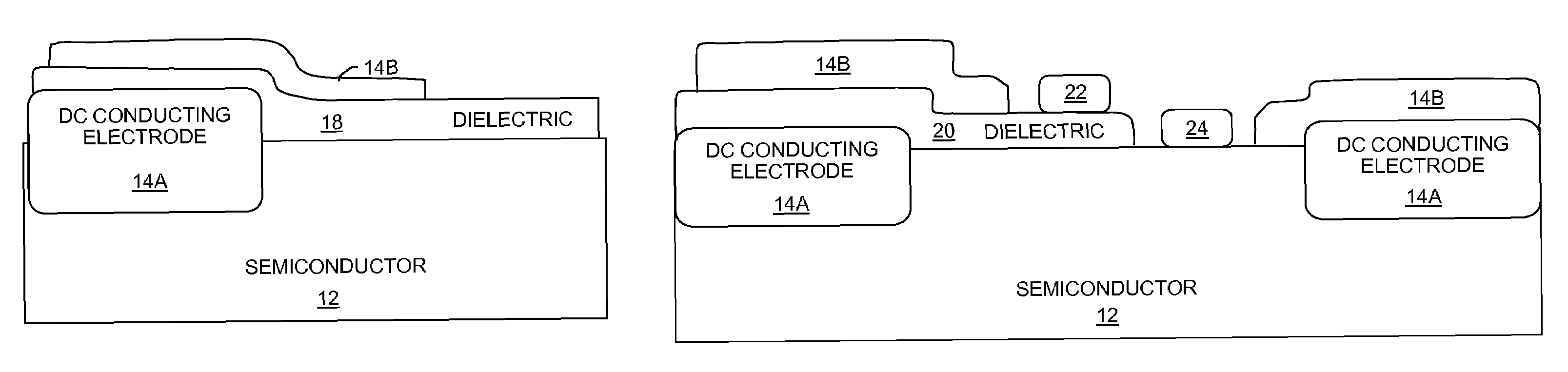
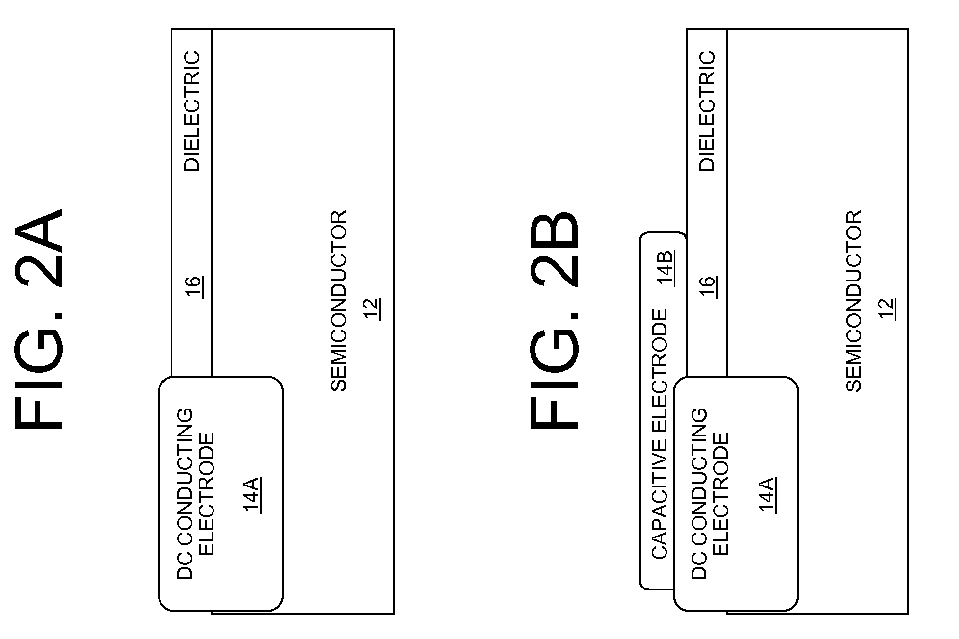
[0020]As indicated above, aspects of the invention provide a method of fabricating a semiconductor device with a composite contact. The fabrication includes forming the composite contact to a semiconductor layer in a semiconductor structure. The composite contact is formed by forming a DC conducting electrode attached to a semiconductor layer in a semiconductor structure and forming a capacitive electrode that is partially over the DC conducting electrode and extends beyond the DC conducting electrode. The composite contact provides a combined resistive-capacitive coupling to the semiconductor layer. As a result, a contact impedance is reduced when the corresponding semiconductor device is operated at high frequencies. As used herein, unless otherwise noted, the term “set” means one or more (i.e., at least one) and the phrase “any solution” means any now known or later developed solution.

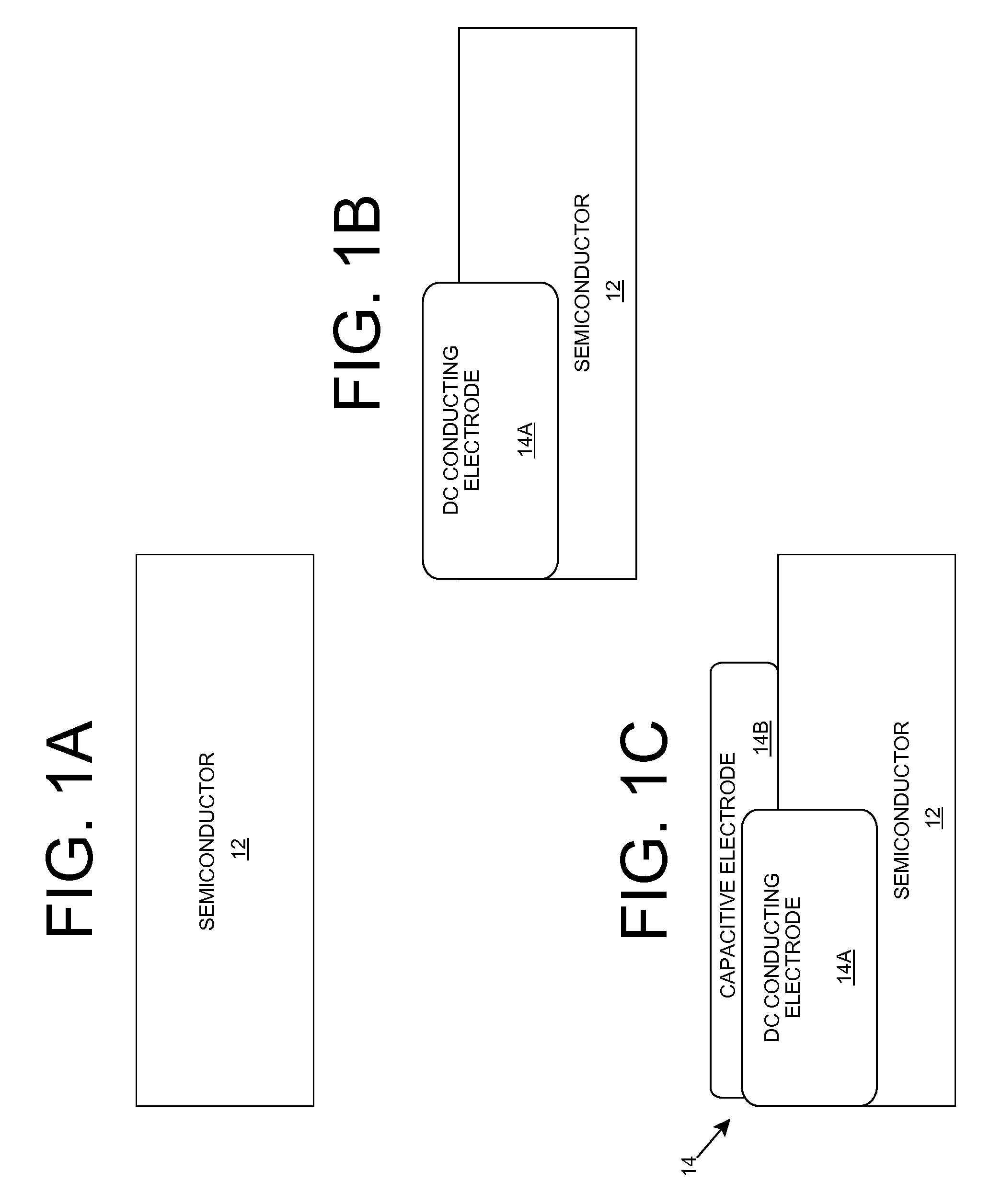
[0021]Turning to the drawings, FIGS. 1A-C show an illustrative composite contact formation accor...


PUM


Abstract

A method of fabricating a semiconductor device with a composite contact is provided. The fabrication includes forming the composite contact to a semiconductor layer in a semiconductor structure. The composite contact is formed by forming a DC conducting electrode attached to a semiconductor layer in a semiconductor structure and forming a capacitive electrode that is partially over the DC conducting electrode and extends beyond the DC conducting electrode. The composite contact provides a combined resistive-capacitive coupling to the semiconductor layer. As a result, a contact impedance is reduced when the corresponding semiconductor device is operated at high frequencies.

Description

REFERENCE TO RELATED APPLICATIONS[0001]The current application claims the benefit of co-pending U.S. Provisional Application No. 60 / 903,109, titled “Method of fabrication of radio-frequency enhanced contacts”, which was filed on 23 Feb. 2007 and U.S. Provisional Application No. 60 / 905,725, titled “Method of fabrication of semiconductor devices with radio-frequency enhanced contacts”, which was filed on 8 Mar. 2007, both of which are hereby incorporated by reference. Aspects of the application are also related to U.S. Provisional Application No. 60 / 903,104, titled “Radio-frequency enhanced contacts to semiconductor devices”, which was filed on 23 Feb. 2007, U.S. Provisional Application No. 60 / 905,634, titled “Radio-frequency enhanced contacts to semiconductor devices”, which was filed on 8 Mar. 2007, and co-pending U.S. Utility application Ser. No. 11 / 781,302, titled “Composite contact for semiconductor device”, which was filed on 23 Jul. 2007, all of which are hereby incorporated by...

Claims


Application Information

Patent Timeline
Patent Type & Authority Patents(United States)
IPC IPC(8): H01L21/338
CPCH01L29/402H01L29/417H01L29/41708H01L29/4175H01L29/41775H01L29/42316H01L29/732H01L29/812H01L29/861H01L29/872
Inventor SIMIN, GRIGORYSHUR, MICHAELGASKA, REMIGIJUS
Owner SENSOR ELECTRONICS TECH
Why Eureka
Try Eureka