Semiconductor device having isolated pockets of insulation in conductive seal ring

a technology of conductive seal ring and isolation pocket, which is applied in the direction of semiconductor devices, semiconductor/solid-state device details, electrical apparatus, etc., can solve the problems of reduced inductance, easy cracks, and easy cracks, and achieve the effect of increasing the yield of the above-mentioned semiconductor devices

Active Publication Date: 2010-03-09
LAPIS SEMICON CO LTD
View PDF14 Cites 9 Cited by
  • Summary
  • Abstract
  • Description
  • Claims
  • Application Information

AI Technical Summary

Benefits of technology

[0020]When a low inductance film is used for the interlayer insulating film of a semiconductor device, the aforementioned seal ring must be formed and the width of this seal ring will be approximately 10 micrometers, extremely large compared to the minute elemental dimensions of 65 nm to 45 nm for semiconductor devices. This is necessary in order to prevent cracks which easily occur in the low inductance film during the dicing process of the semiconductor chip and during the CMP process for forming the damascene wiring structure. Note, when these cracks occur, there will be problems with moisture penetrating into the low inductance film as previously described. These cracks easily occur when the inductance is reduced in low inductance films. This is because the mechanical strain of the interlayer insulating film is inevitably reduced when reducing the inductance. Furthermore, these cracks easily occur when the semiconductor chip area is increased and when multiple layers of damascene wiring structures are used. Therefore, miniaturizing of this seal ring width has not progressed along with miniaturizing of the element structure of the semiconductor device.
[0021]Therefore, when a seal ring 102 is formed as described above wherein at least one part has a damascene wiring structure, a bridge region 123 will form at a certain frequency between the electrode pad and the groove wiring which is adjacent to the seal ring 102. When this type of bridge region occurs, the groove wiring or electrode pad of the element forming region will be electrically shorted to the seal ring 102 and the groove wiring or the electrode pad of the semiconductor device will cease to function. Furthermore, in the manufacturing process of the semiconductor device, fewer proper semiconductor chips will be produced and the yield of the semiconductor devices will be reduced. Furthermore, the occurrence of these bridge regions will become more dramatic as the number of layers of damascene wiring increases,
[0027]With the structure of the present invention, electrical shorts between the seal ring which contains a damascene wiring structure and the groove wiring which is adjacent to the seal ring or the electrode pad can be prevented, thus increasing the yield of the aforementioned semiconductor devices.

Problems solved by technology

Note, when these cracks occur, there will be problems with moisture penetrating into the low inductance film as previously described.
These cracks easily occur when the inductance is reduced in low inductance films.
Furthermore, these cracks easily occur when the semiconductor chip area is increased and when multiple layers of damascene wiring structures are used.
Therefore, miniaturizing of this seal ring width has not progressed along with miniaturizing of the element structure of the semiconductor device.
Furthermore, in the manufacturing process of the semiconductor device, fewer proper semiconductor chips will be produced and the yield of the semiconductor devices will be reduced.

Method used


Image

  • Semiconductor device having isolated pockets of insulation in conductive seal ring
  • Semiconductor device having isolated pockets of insulation in conductive seal ring
  • Semiconductor device having isolated pockets of insulation in conductive seal ring

Examples


Embodiment Construction

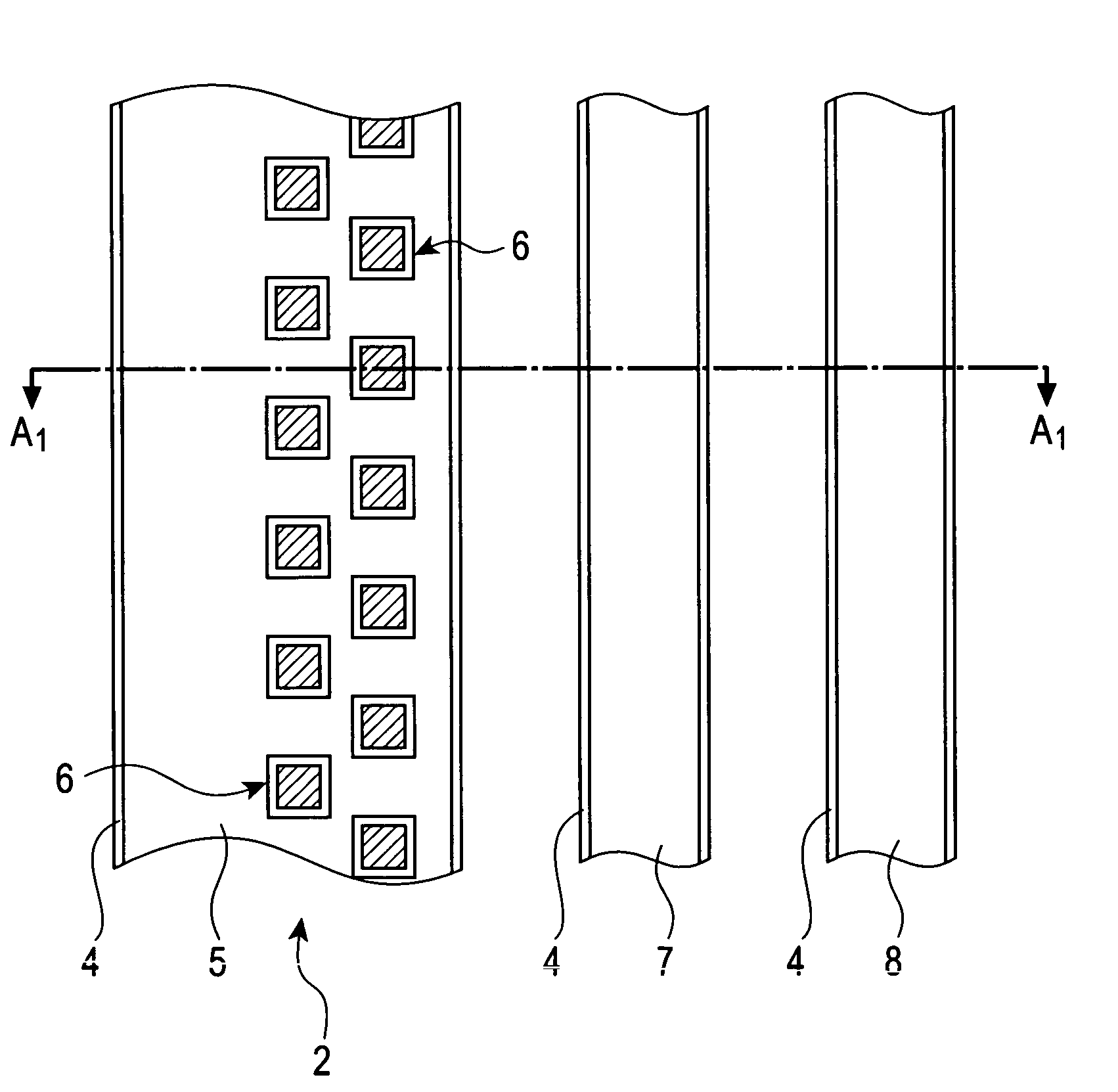
[0037]A preferred embodiment of the present invention will be described below while referring to the drawings. In this description, objects which are common to all drawings are assigned the same reference numerals. FIG. 5 is a top view drawing of a semiconductor chip which has a two-dimensional arrangement on a semiconductor wafer, FIG. 6 is a partial enlarged drawing of the surrounding edge of a semiconductor chip, FIG. 7 is a cross-section view of the seal ring region of the present invention, and FIG. 8A through FIG. 8C are element cross-section views by manufacturing process for the seal ring region of the present invention.

[0038]As shown in FIG. 5, a seal ring 2 is formed along the outside edge of a semiconductor chip 1 so as to enclose an element forming region. A partial enlargement of this region 3 is shown in FIG. 6. The seal ring 2 of this embodiment is formed by connecting multiple overlaying layers of the same material which makes up the wiring and via plug of the semico...


PUM


Abstract

A semiconductor device with a damascene wiring structure which can prevent short-circuits between a seal ring and a wiring line or electrode pad. An upper layer barrier layer made from a conductive barrier material film is formed on an interlayer insulating film groove sidewall of the semiconductor device. Embedded in the groove is an upper layer seal ring wiring line with thickness of approximately 10 micrometers for instance, in which a plurality of isolated pockets of insulators are disbursed. These isolated pockets of insulators are formed using the interlayer insulating film which forms the damascene wiring line. Additionally, a first upper layer groove wiring line and a second upper layer groove wiring line are formed in an element forming region, and an upper layer barrier layer is formed on the outside perimeter. The upper layer seal ring wiring line and both upper layer wiring lines all have damascene wiring structures.

Description

BACKGROUND OF THE INVENTION[0001]1. Field of the Invention[0002]The present invention relates to a semiconductor device, and in particular relates to a semiconductor device which has a damascene wiring structure.[0003]2. Description of the Related Art[0004]Miniaturizing of the elements which form semiconductor devices is most effective for increasing the performance of the semiconductor device, and currently, the design standards for this dimension are shifting from 65 nm to 45 nm, and technology development is vigorously being promoted. Furthermore, in order to increase the performance of semiconductor devices having miniaturized structures, a groove wiring line formed by the so-called damascene method, or in other words, a damascene wiring line is necessary, wherein a wiring material layer such as a copper (Cu) layer is deposited onto an interlayer insulating layer which has grooves formed by minute machining and the wiring material layer region that is not embedded in the grooves...

Claims


Application Information

Patent Timeline
Patent Type & Authority Patents(United States)
IPC IPC(8): H01L23/48
CPCH01L23/585H01L2924/0002H01L2924/00
Inventor TOKITOH, SHUNICHIKONDOU, SEIICHIYOON, BO UN
Owner LAPIS SEMICON CO LTD
Why Eureka
Try Eureka