Semiconductor device
a technology of semiconductor devices and semiconductor elements, applied in semiconductor devices, semiconductor/solid-state device details, electrical apparatus, etc., can solve the problems of physical damage to semiconductor elements and degraded characteristics, and achieve the effect of simple and low-cost processes
- Summary
- Abstract
- Description
- Claims
- Application Information
AI Technical Summary
Benefits of technology
Problems solved by technology
Method used
Image

Examples
first embodiment
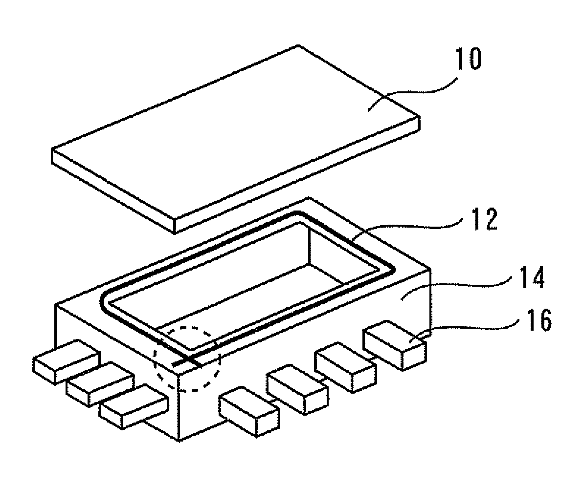
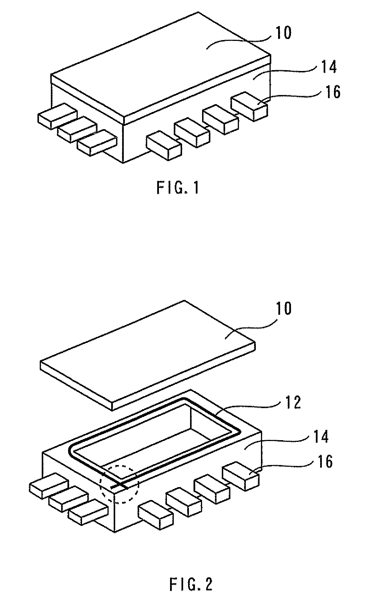
[0031]FIG. 1 is a perspective view illustrating the configuration of a semiconductor device according to a first embodiment of the present invention. This semiconductor device includes a package case 14 which is a box-like container having at least one open side. A cap 10 is disposed to cover this open side. The cap 10 is bonded to the package case 14 so as to hermetically seal the inside of the package case 14 or the package.
[0032]FIG. 2 is a perspective view illustrating in detail a method for bonding the cap 10 to the package case 14 in accordance with the present invention. Specifically, FIG. 2 shows the package case 14 and the cap 10 before they are bonded together. As shown, the package case 14 has one open side. Though not shown, a semiconductor element is mounted at a predetermined position on an inner wall of the package case 14 through this open side. It should be noted that the semiconductor element mounted in the package case 14 is of the type that need be protected from...
second embodiment
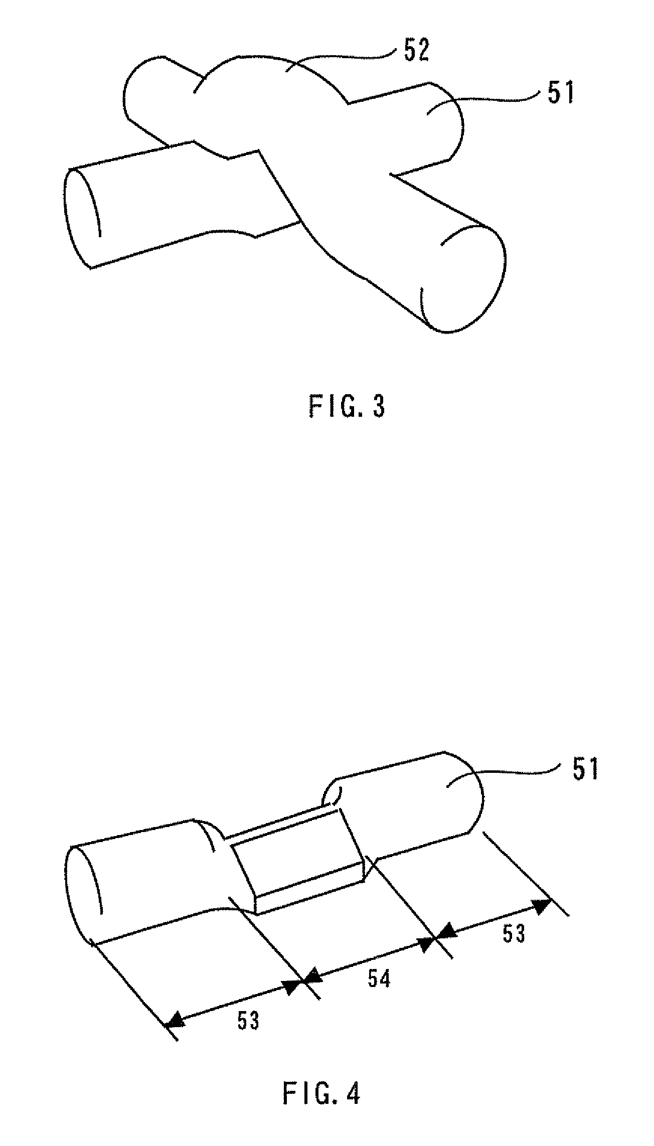
[0046]A second embodiment of the present invention provides a semiconductor device in which a semiconductor element is reliably hermetically sealed within a package, and provides a method for manufacturing such a semiconductor device. The following description of the present embodiment will be directed only to the differences from the first embodiment. FIG. 8A is a perspective view illustrating the configuration of the semiconductor device of the present embodiment. This semiconductor device includes eight bonding / sealing wires, namely, bonding / sealing wires 40, 42, 44, 46, 48, 50, 60, and 62. Each pair of these eight bonding / sealing wires are disposed on and along a respective side of the rim of the open side of a package case 14 (i.e., the bonding / sealing wires of each pair extend parallel to each other). The ends of the eight bonding / sealing wires cross one another, as shown in FIG. 8A, so that the bonding / sealing wires together form two concentric closed loops.
[0047]FIG. 8B is a...
third embodiment
[0051]A third embodiment of the present invention provides a semiconductor device in which the package case and the cap are firmly bonded together, and provides a method for manufacturing such a semiconductor device. The following description of the present embodiment will be directed only to the differences from the first embodiment. FIG. 9 is a diagram illustrating the configuration of the semiconductor device of the present embodiment. Specifically, FIG. 9 shows its package case 14 and cap 10 before they are bonded together. The semiconductor device of the present embodiment includes bonding / sealing wires 70, 72, 74, and 76. Each bonding / sealing wire is disposed on a respective side of the rim of the open side of the package case 14, as shown in FIG. 9. (The cap 10 is bonded to the rim of the package case 14 by the bonding / sealing wires.) It should be noted that before the cap 10 is bonded to the package case 14, the adjacent ends of each adjacent pair of these bonding / sealing wi...
PUM
 Abstract
Description
Claims
Application Information
 - R&D
- Intellectual Property
- Life Sciences
- Materials
- Tech Scout
- Unparalleled Data Quality
- Higher Quality Content
- 60% Fewer Hallucinations
Browse by: Latest US Patents, China's latest patents, Technical Efficacy Thesaurus, Application Domain, Technology Topic, Popular Technical Reports.
© 2025 PatSnap. All rights reserved.Legal|Privacy policy|Modern Slavery Act Transparency Statement|Sitemap|About US| Contact US: help@patsnap.com