Method of fabricating semiconductor device

a semiconductor device and manufacturing method technology, applied in semiconductor devices, semiconductor/solid-state device details, electrical equipment, etc., can solve the problems of inability to improve the performance and reliability of io devices, the nbti of io pmos cannot be reduced, and the manpower is profitless to the so as to increase the performance and reliability of io pmos, prevent the diffusion of hydrogen atoms, and simple manufacturing steps

Active Publication Date: 2010-03-23
UNITED MICROELECTRONICS CORP
View PDF11 Cites 2 Cited by
  • Summary
  • Abstract
  • Description
  • Claims
  • Application Information

AI Technical Summary

Benefits of technology

[0006]Accordingly, a main objective of the present invention is to provide a method of fabricating a semiconductor device capable of increasing the performance and reliability of a IO PMOS through simple manufacturing steps and preventing the diffusion of hydrogen atoms into the interface between silicon (Si) and silicon dioxide (SiO2). The method has very little impact on the resistance (Rs) of the metal silicide layer.
[0007]Another main objective of the present invention is to provide a semiconductor device capable of eliminating the negative bias temperature instability (NBTI) in a IO PMOS so that the performance and the reliability of the device are improved.
[0018]In the present invention, a thin buffer layer is formed on the surface of the IO PMOS, and the buffer layer can stop the diffusion of hydrogen atoms into the interface between silicon and silicon oxide. Hence, the negative bias temperature instability (NBTI) of the IO PMOS can be eliminated or reduced without affecting the performance of other devices. Moreover, the buffer layer has very little impact on the resistance (Rs) of the underlying metal silicide layer.

Problems solved by technology

The use of strained silicon has been utilized to improve the performance of the core device, but this manner is profitless to the reliability of a IO PMOS.
Furthermore, the higher voltage is applied to the IO devices, especially the IO PMOS, so NBTI of the IO PMOS can not be reduced and thus the performance and reliability of the IO devices cannot be improved.

Method used


Image

  • Method of fabricating semiconductor device
  • Method of fabricating semiconductor device
  • Method of fabricating semiconductor device

Examples


Embodiment Construction

[0023]Reference will now be made in detail to the present preferred embodiments of the invention, examples of which are illustrated in the accompanying drawings. Wherever possible, the same reference numbers are used in the drawings and the description to refer to the same or like parts.

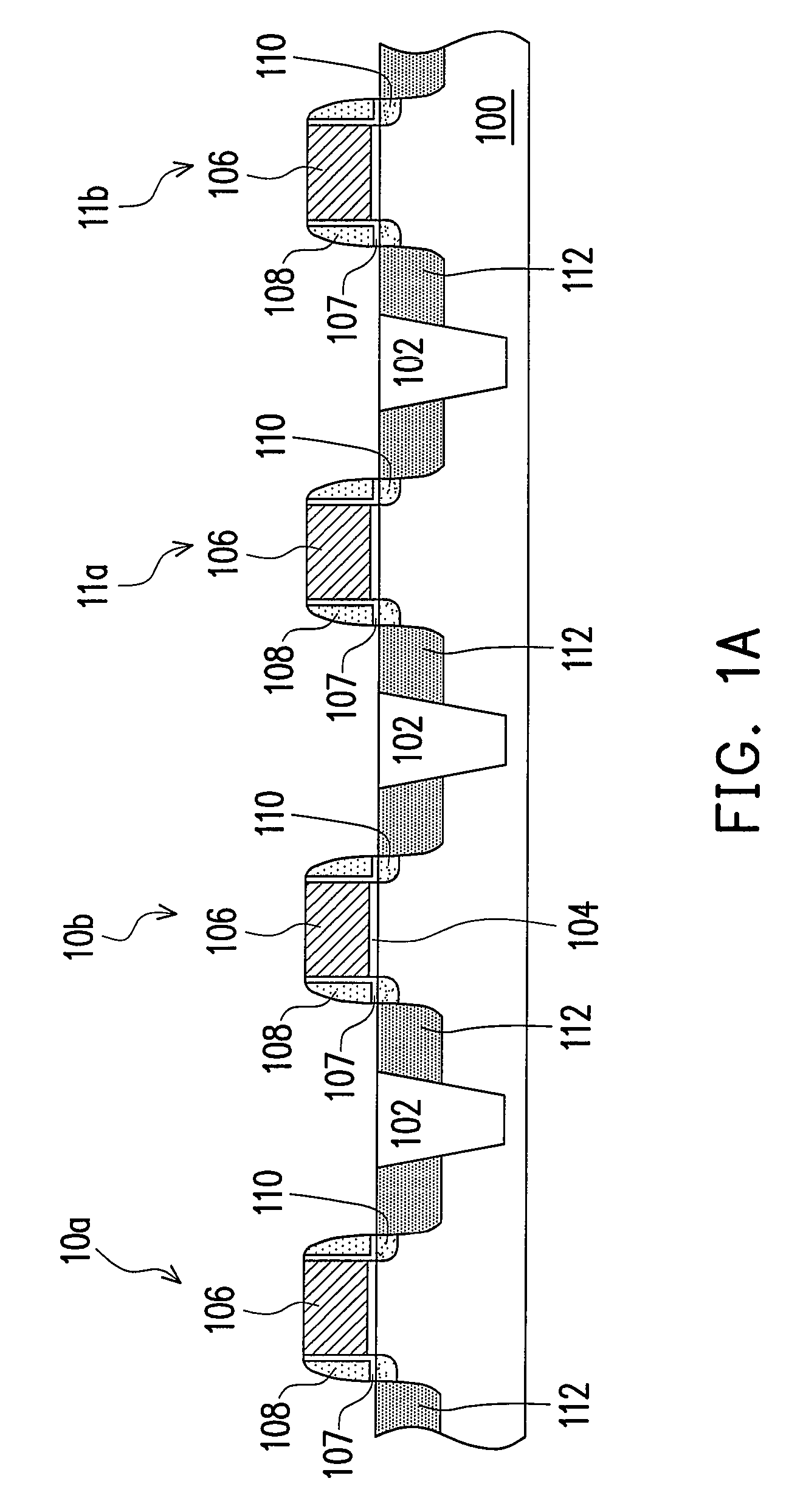
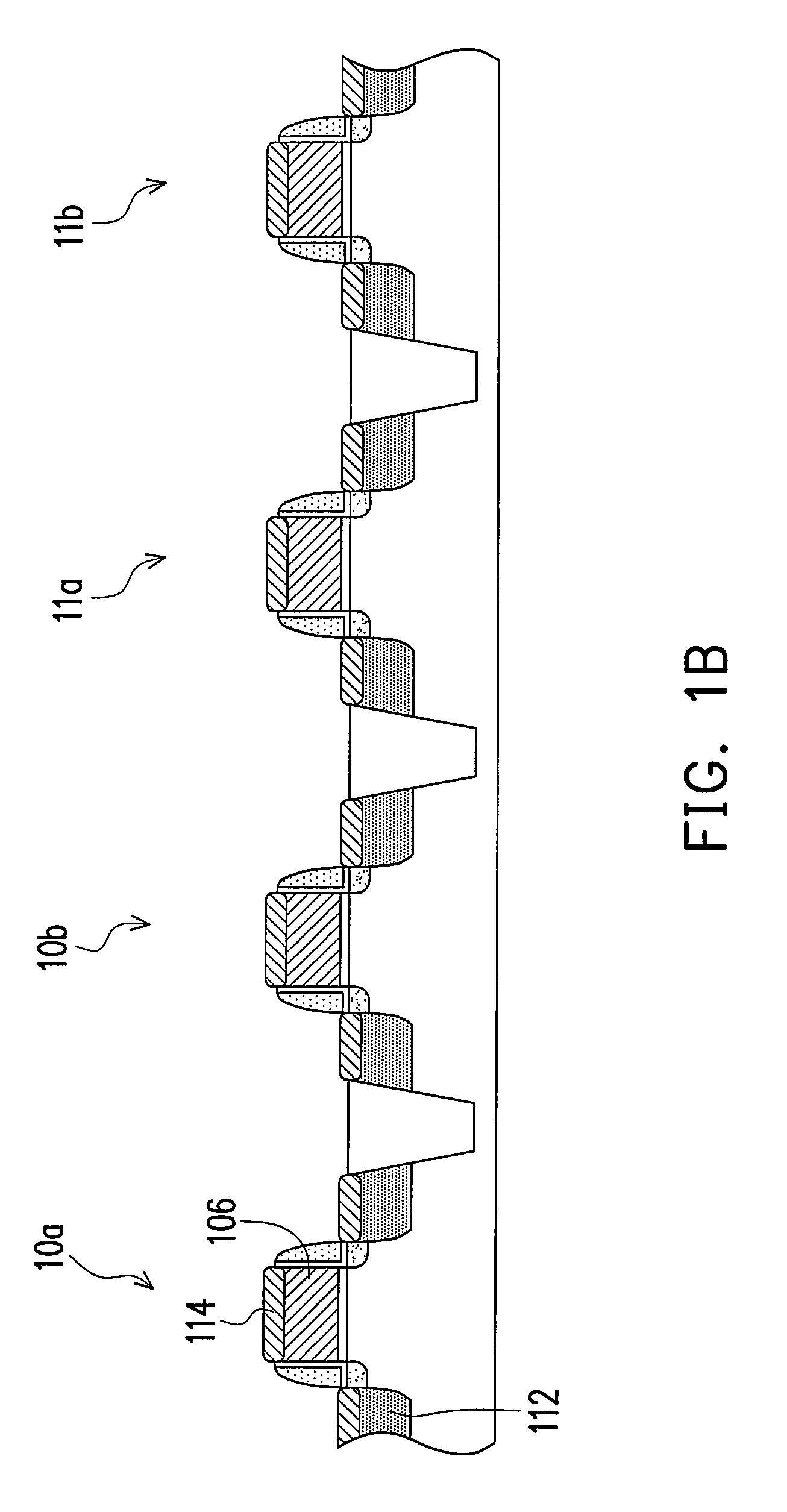
[0024]FIGS. 1A through 1D are schematic cross-sectional views showing the steps for fabricating a semiconductor device according to one preferred embodiment of the present invention.

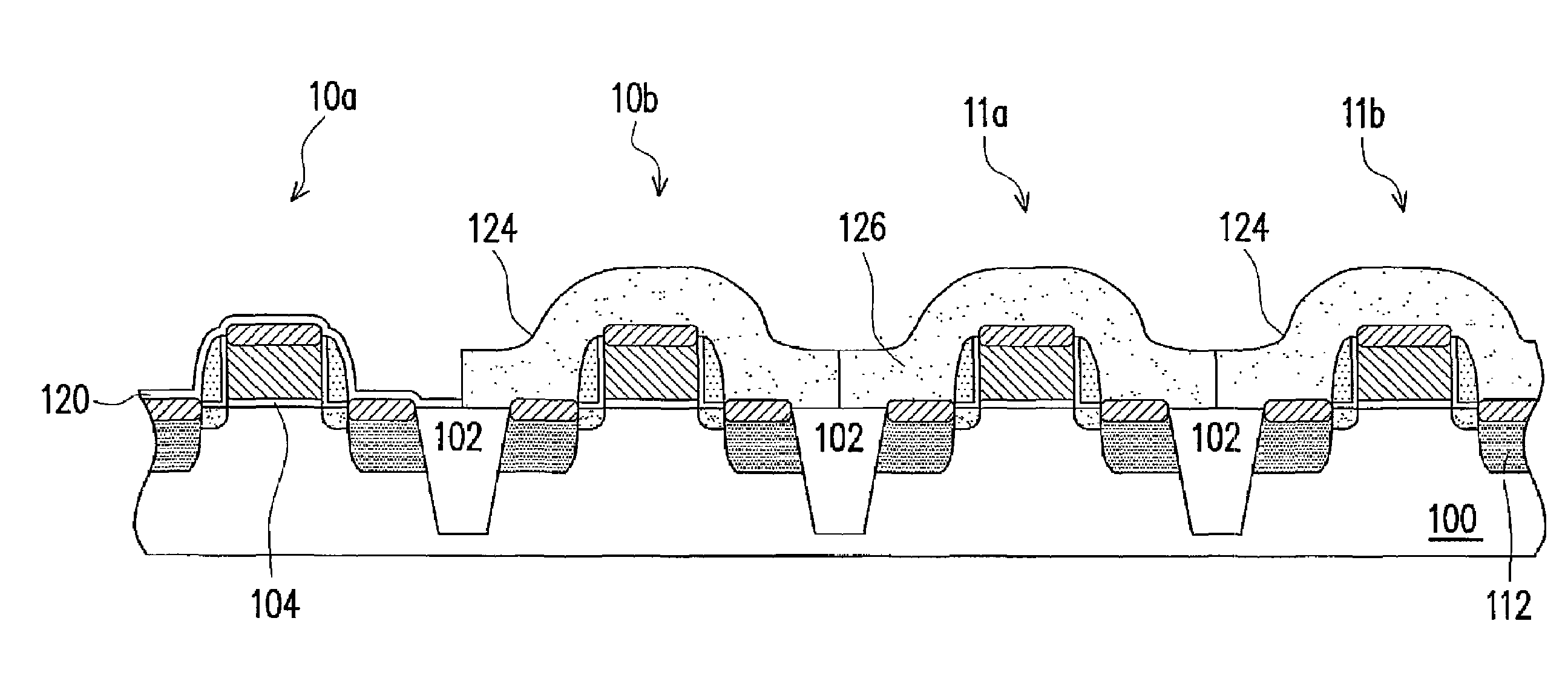
[0025]As shown in FIG. 1A, a substrate 100 with multiple isolation structures 102 is provided. Several IO devices 10a and 10b and several core devices 11a and 11b are formed on the substrate 100. The IO devices include a IO PMOS 10a and a IO NMOS 10b, and The core devices include a core PMOS 11a and a core NMOS 11b. The core device 11a and 11b, the IO PMOS 10a and the IO NMOS 10b respectively comprise a metal-semiconductor-oxide at least including a gate dielectric layer 104, a gate 106, a spacer 108, a lightly doped drai...


PUM


Abstract

A method of fabricating a semiconductor device is provided. A substrate is first provided, and then several IO devices and several core devices are formed on the substrate, wherein those IO devices include IO PMOS and IO NMOS, and those core devices include core PMOS and core NMOS. Thereafter, a buffer layer is formed on the substrate, and then the buffer layer except a surface of the IO PMOS is removed in order to reduce the negative bias temperature instability (NBTI) of the IO PMOS. Afterwards, a tensile contact etching stop layer (CESL) is formed on the IO NMOS and the core NMOS, and a compressive CESL is formed the core PMOS.

Description

BACKGROUND OF THE INVENTION[0001]1. Field of the Invention[0002]The present invention relates to a semiconductor device and a method of fabricating thereof. More particularly, the present invention relates to a semiconductor device and fabricating method thereof capable of improving negative bias temperature instability (NBTI) of the PMOS used as a input / output (IO) device.[0003]2. Description of the Related Art[0004]In the matter of the function, the semiconductor devices can be mainly distributed into IO devices and core devices. In accordance with electrical type of the devices, the IO devices further include a IO PMOS and a IO NMOS, wherein the IO PMOS represents a PMOS used as a IO device and the IO NMOS represents a NMOS used as a IO device. The core devices similarly include a core PMOS and a core NMOS.[0005]The use of strained silicon has been utilized to improve the performance of the core device, but this manner is profitless to the reliability of a IO PMOS. Furthermore, t...

Claims


Application Information

Patent Timeline
Patent Type & Authority Patents(United States)
IPC IPC(8): H01L21/336H01L21/8234H01L21/8238
CPCH01L21/823807H01L29/7843H01L29/665H01L29/6656
Inventor HUNG, WEN-HANHUANG, CHENG-TUNGJENG, LI-SHIANLEE, KUN-HSIENTING, SHYH-FANNCHENG, TZYY-MINGLIANG, CHIA-WEN
Owner UNITED MICROELECTRONICS CORP
Why Eureka
Try Eureka