Intelligent dead time control

a dead time control and intelligent technology, applied in the direction of electric variable regulation, process and machine control, instruments, etc., can solve the problems of power loss, delay between control, and the inability of the dead time itself to achieve the optimum delay, so as to achieve the effect of optimum dead time and power loss reduction

Active Publication Date: 2010-03-23
INFINEON TECH AMERICAS CORP
View PDF10 Cites 32 Cited by
  • Summary
  • Abstract
  • Description
  • Claims
  • Application Information

AI Technical Summary

Benefits of technology

[0012]It is an object of the present invention to provide an improved solution to providing a fixed delay for any type of rectifier / Power Device by comparing low side gate drive and switch node / high side gate drive edges to achieve optimum dead time to reduce power losses.
[0013]It is a further object of the present invention to reduce or eliminate any conduction, reverse recovery, and / or shoot through loss.
[0014]A circuit is provided for reducing switching losses in a synchronous rectifier or a switching stage including a high-side control transistor and a low-side synchronous transistor coupled at a switching node, the switching stage receiving an input voltage and providing a controlled output voltage at an output node. The circuit includes a first circuit portion for sensing waveshape edges of a first signal at a gate terminal of the low-side synchronous transistor and a first voltage to determine a delay between the waveshape edge of the first signal and the waveshape edge of the first voltage; and a second circuit portion for calibrating the first signal and the first voltage to align the waveshape edge of the first signal and the waveshape edge of the first voltage.

Problems solved by technology

In synchronous rectifiers, one of the main contributors of the power losses is the delay between the control of a high-side / control transistor and the low side / synchronous transistor.
The dead time itself cannot be adjusted to achieve the optimum delay per given conditions.
Due to VSW comparator delay, this approach does not achieve optimum dead time.

Method used


Image

  • Intelligent dead time control
  • Intelligent dead time control
  • Intelligent dead time control

Examples


Embodiment Construction

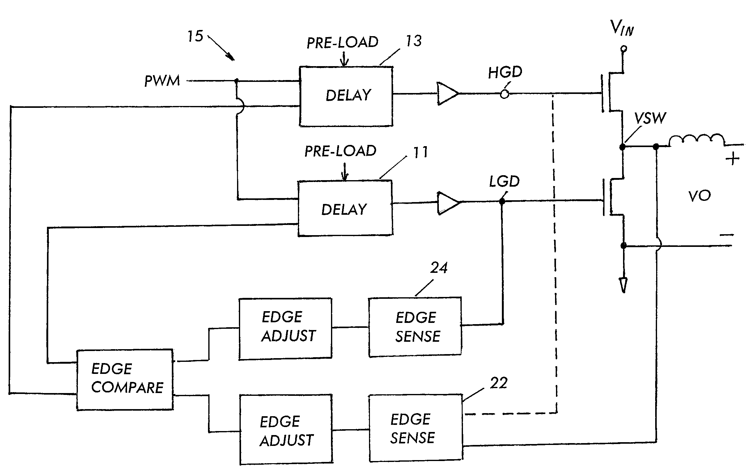
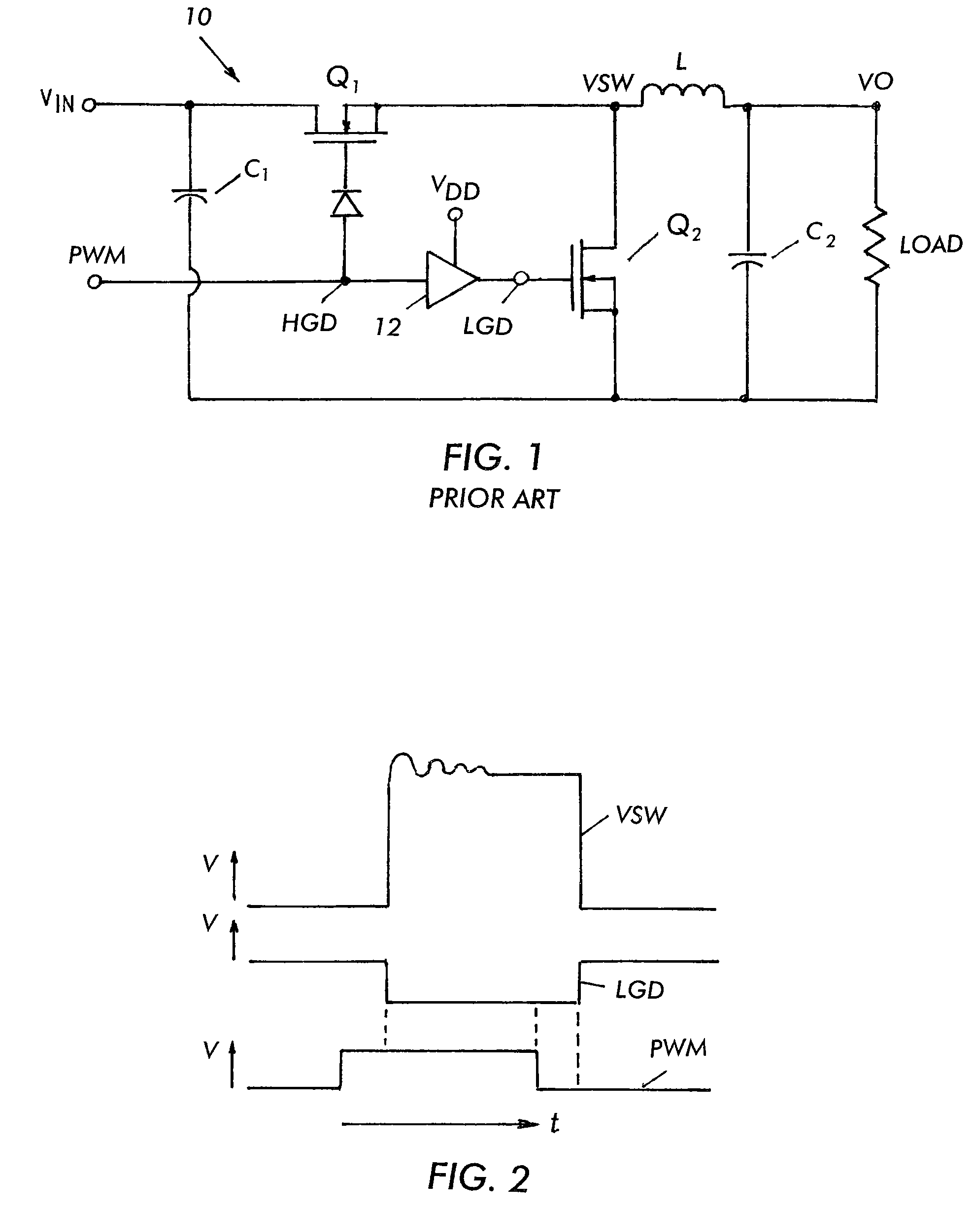
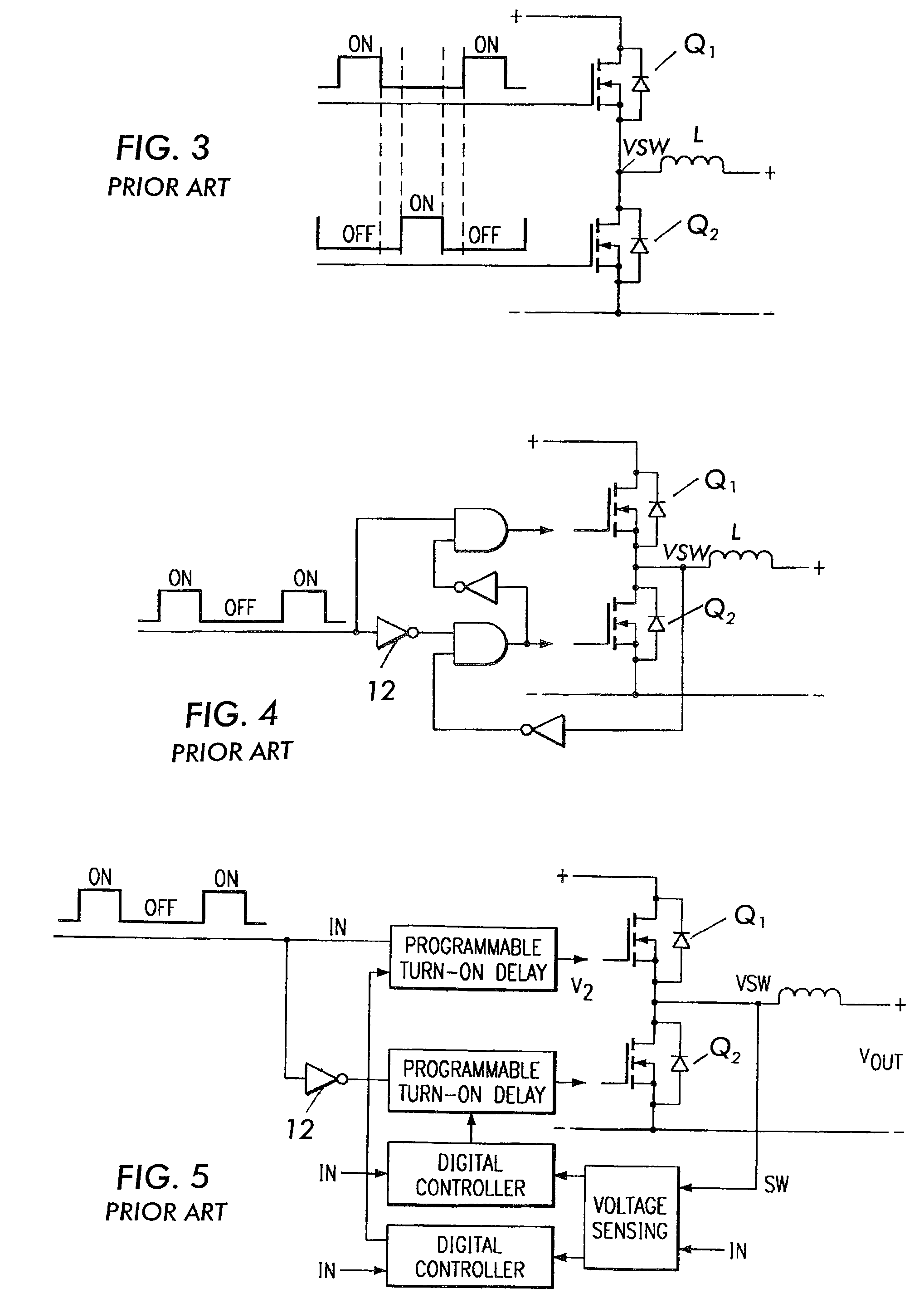
[0025]FIG. 1 shows a PWM input to gates of high- and low-side transistors Q1 and Q2. The signal to the high-side transistor Q1 is identified as HGD and the signal to the low-side transistor Q2 is inverted by an inverter 12 and identified as LGD, having a waveshape LGD shown in FIG. 2. The high- and low-side transistors Q1 and Q2 are connecting at a switching node.

[0026]FIG. 2 illustrates, rising and falling edges of the waveshape of the signal LGD aligned with rising and falling edges of a waveshape of a voltage VSW at the switching node and / or a waveshape of the signal HGD.

[0027]Returning to FIG. 1, in accordance with the invention, in a high speed synchronous buck converter where the low-side transistor Q2 is made to switch very fast, for example, within one nanosecond, the optimum dead time occurs when a gate signal of the low-side transistor Q2 is aligned with the rise / fall edges of a waveform of the voltage VSW and / or the signal HGD.

[0028]The synchronization of the waveshape ed...


PUM


Abstract

A circuit for reducing switching losses in a synchronous rectifier of a switching stage including a high-side control transistor and a low-side synchronous transistor coupled at a switching node, the switching stage receiving an input voltage and providing a controlled output voltage at an output node. The circuit including a first circuit portion for sensing waveshape edges of a first signal at a gate terminal of the low-side synchronous transistor and a first voltage to determine a delay between the waveshape edge of the first signal and the waveshape edge of the first voltage; and a second circuit portion for calibrating the first signal and the first voltage to align the waveshape edge of the first signal and the waveshape edge of the first voltage, with an optional offset to achieve minimal power loss.

Description

BACKGROUND OF THE INVENTION[0001]1. Field of the Invention[0002]This invention relates to converter circuits and more specifically to a control circuit for reducing the dead time between conduction of high side and low side FETs in such circuit.[0003]2. Description of the Related Art[0004]In DC to DC conversion, “good converters” are measured according to the converter efficiency. Efficiency is determined in accordance with fewest power losses in the converters, such as switching losses and losses due to the Power Device's ON resistance.[0005]Synchronous rectifiers are commonly used to reduce switching losses, despite their control complexity. In synchronous rectifiers, one of the main contributors of the power losses is the delay between the control of a high-side / control transistor and the low side / synchronous transistor.[0006]FIG. 1 illustrates a well-known high-speed synchronous buck converter circuit 10. The circuit 10 includes a switching stage having a high side or control Po...

Claims


Application Information

Patent Timeline
Patent Type & Authority Patents(United States)
IPC IPC(8): G05F1/40
CPCH02M1/38H02M7/219H02M1/08H02M3/155
Inventor KIM, SEUNGBEOM KEVINVACCA, TODDZHANG, JASON
Owner INFINEON TECH AMERICAS CORP
Why Eureka
Try Eureka