Substrate-processing apparatus with buffer mechanism and substrate-transferring apparatus

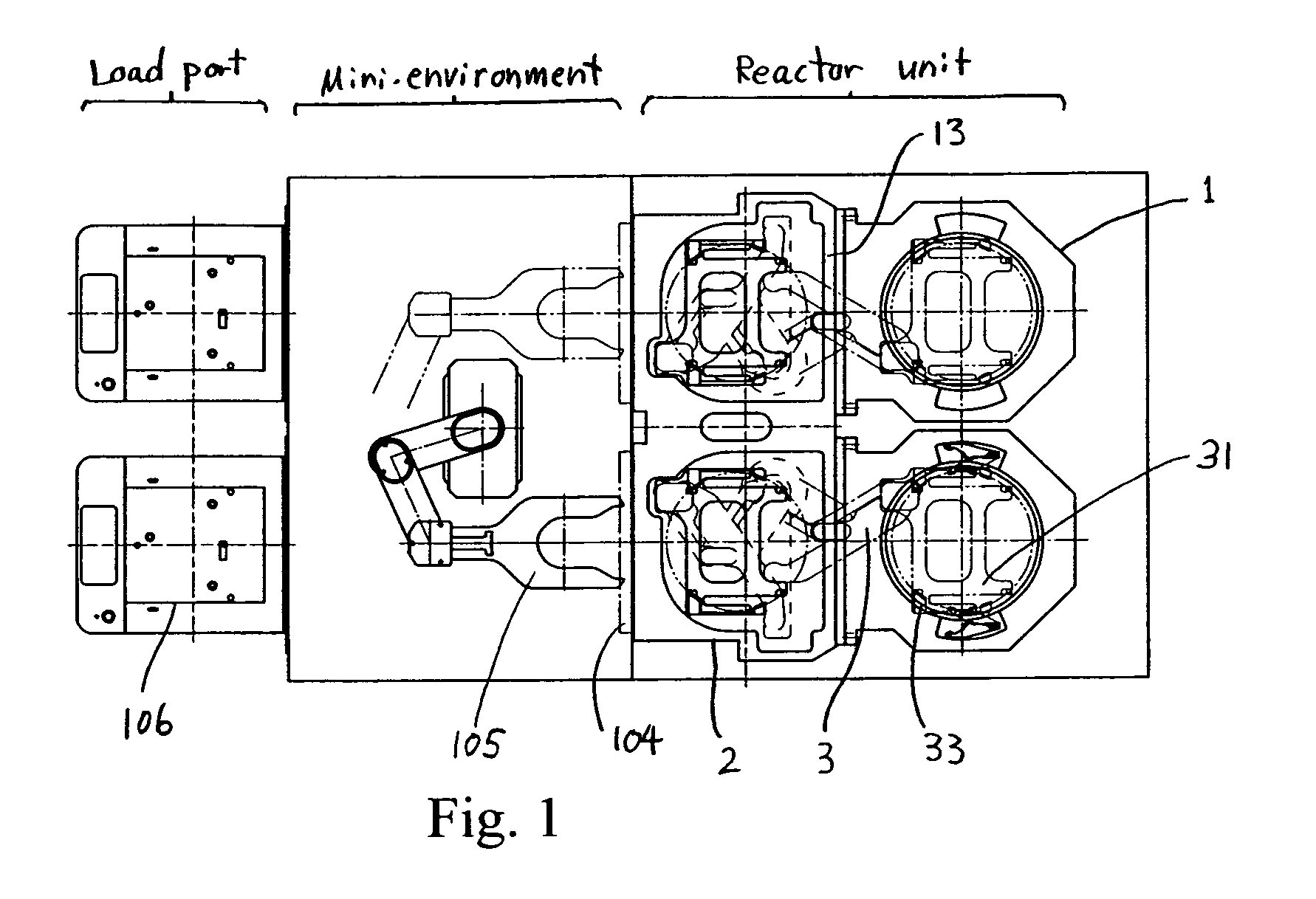
a substrate-transferring apparatus and substrate-processing technology, which is applied in the direction of tableware, furnaces, hoisting equipment, etc., can solve the problems of increasing the number of reactors, the occurrence of non-uniform film thickness and film quality of thin film formed on a wafer, and the increase of the footprint (apparatus space required) and the faceprint (the panel width of the apparatus front). , the effect of small footprint and low cos

Active Publication Date: 2010-04-06
ASM JAPAN
View PDF17 Cites 388 Cited by
  • Summary
  • Abstract
  • Description
  • Claims
  • Application Information

AI Technical Summary

Benefits of technology

[0011]Accordingly, in an embodiment of the present invention, provided is a substrate-processing apparatus that realizes low costs, a small footprint and a small faceprint.
[0012]Further, in an embodiment of the present invention, provided is a substrate-processing apparatus that realizes stable processes and high throughput.
[0016]In an embodiment, the reaction chamber is provided with a buffer mechanism for buffering or temporarily supporting a processed substrate or an unprocessed substrate. The buffer mechanism of the reaction chamber cooperates with the transferring arm with the dual end-effectors. Even though a single arm is used for one reaction chamber, by using the single arm provided with multiple end-effectors and the buffer mechanism of the reaction chamber, transferring capacity can be greater than when dual arms are used, and the size of the load-lock chamber can be small. Further, throughput can significantly be high.

Problems solved by technology

In batch processing, the occurrence of non-uniformity of film thickness and film quality of a thin film formed on a wafer frequently becomes a problem.
In order to increase productivity using a conventional single-wafer-processing type processing apparatus, the number of reactors increases, a footprint (apparatus space required) and a faceprint (the panel width of a apparatus front) increase, and costs run up.
Additionally, due to the increase in the number of reactors, output significantly drops if operation discontinues due to apparatus breakdowns or maintenance.
Furthermore, in the thin film deposition process, it is often the case that process time is short and the processes are performed consecutively.
If equipping the wafer transferring mechanism with the double arms, the transferring mechanism complexifies and costs run up.
Additionally, the capacity of the load-lock chamber increases, hence time required for evacuating air and time required for restoring to atmospheric pressure are lengthened and transfer rate-limiting factors increase.
As a result, throughput is restricted.
Furthermore, even in an apparatus using a regular polygonal type transfer chamber, for the purpose of carrying in and out wafers inside the reactor efficiently, although the wafer transferring mechanism having double arms is better, the transferring mechanism complexities and costs run up.

Method used


Image

  • Substrate-processing apparatus with buffer mechanism and substrate-transferring apparatus
  • Substrate-processing apparatus with buffer mechanism and substrate-transferring apparatus
  • Substrate-processing apparatus with buffer mechanism and substrate-transferring apparatus

Examples


Embodiment Construction

[0034]The invention will be explained in detail below with reference to preferred embodiments. However, the preferred embodiments are not intended to limit the present invention.

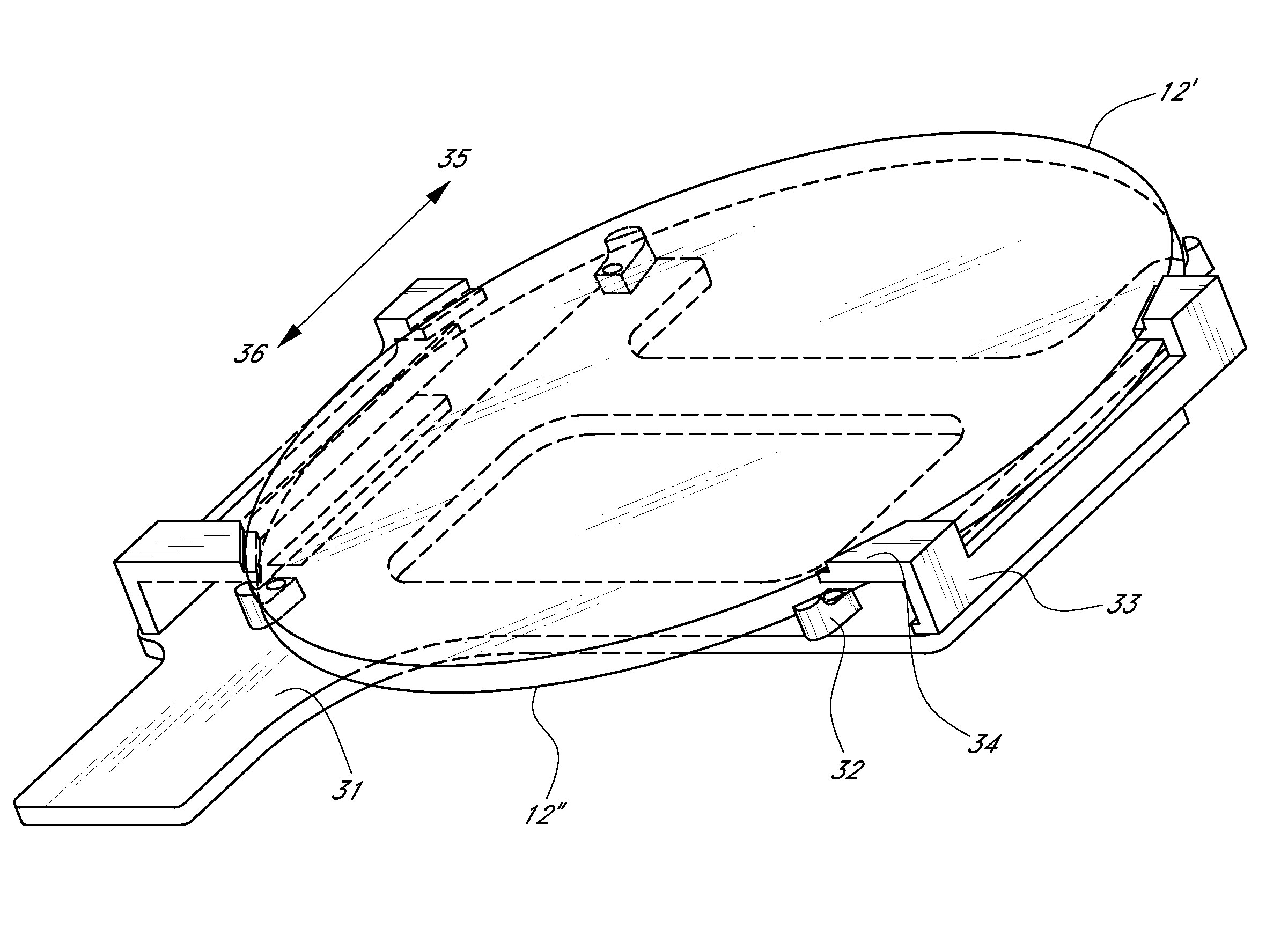
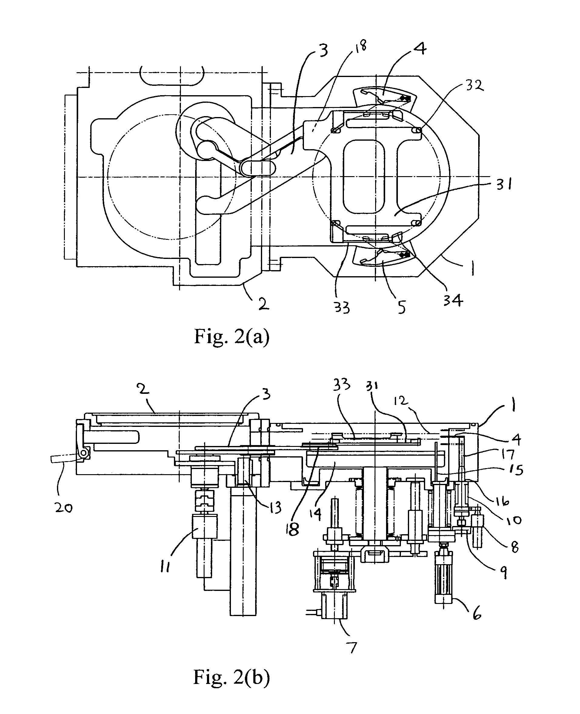
[0035]1) A substrate transfer apparatus for loading and unloading substrates in a reaction chamber may comprise: (a) an arm having a distal end which is laterally movable in a straight line direction; and (b) end-effectors for loading and unloading substrates in a reaction chamber, which include a lower end-effector and an upper end-effector, wherein one of the lower end-effector or the upper end-effector is movably coupled to the arm at the distal end of the arm, and the other of the lower end-effector or the upper end-effector is fixed to the movably coupled end-effector, wherein the movably coupled end-effector has a front side, rear side, right side, and left side, and the fixed end-effector is comprised of multiple portions which are fixed to the movably coupled end-effector exclusively at the right and...


PUM


Abstract

A substrate transfer apparatus for loading and unloading substrates in a reaction chamber, includes: an arm having a distal end which is laterally movable in a straight line direction; and end-effectors for loading and unloading substrates in a reaction chamber, which include a lower end-effector and an upper end-effector. One of the lower end-effector or the upper end-effector is movably coupled to the arm at a distal end of the arm, and the other end-effector is fixed to the movably coupled end-effector. The fixed end-effector is fixed to the movably coupled end-effector.

Description

BACKGROUND OF THE INVENTION[0001]1. Field of the Invention[0002]The present invention relates to a substrate-processing apparatus using a vacuum load-lock system and a substrate-transferring apparatus. The invention further relates to a buffer mechanism for buffering semiconductor substrates.[0003]2. Description of the Related Art[0004]Generally, chambers of a semiconductor-processing apparatus using a vacuum load-lock system, which is used for manufacturing conventional semiconductor integrated circuits, comprise a load-lock chamber, a transfer chamber and multiple reactors (process chambers) connected to the transfer chamber. For each chamber, a wafer transfer robot is used for supplying wafers automatically. The semiconductor-processing apparatus using a vacuum load-lock system operates in the following manner: First, an atmospheric robot carries a wafer from a cassette or a front opening unified pod (“FOUP”, e.g., a box possessing detachable cassettes and a front opening interfa...

Claims


Application Information

Patent Timeline
Patent Type & Authority Patents(United States)
IPC IPC(8): B65G49/07
CPCH01L21/67196H01L21/68707H01L21/67745H01L21/67201Y10S294/902Y10S414/141H01L21/67742
Inventor YAMAGISHI, TAKAYUKIKOBAYASHI, TAMIHIROWATANABE, AKIRAKANEUCHI, KUNIHIRO
Owner ASM JAPAN
Why Eureka
Try Eureka