High voltage GaN transistors

a high-voltage gan transistor and transistor technology, applied in the field of semiconductors, can solve the problems of low electron mobility, low electron mobility, and high source resistance, and achieve the effect of limiting the performance of these devices, and the difference between dc and rf characteristics

Active Publication Date: 2010-04-06
CREE INC
View PDF50 Cites 107 Cited by
  • Summary
  • Abstract
  • Description
  • Claims
  • Application Information

AI Technical Summary

Problems solved by technology

One disadvantage of Si is that it has low electron mobility (600-1450 cm2 / V-s), which produces a high source resistance that can degrade high performance gain [CRC Press, The Electrical Engineering Handbook, Second Edition, Dorf, p.
Electron trapping and the resulting differences between DC and RF characteristics have been a limiting factor in the performance of these devices.
Due to the high electric fields existing in these structures, however, charge trapping is still an issue.
The approaches known in the art, however, have limitations for high performance applications in power switching.

Method used


Image

  • High voltage GaN transistors
  • High voltage GaN transistors
  • High voltage GaN transistors

Examples


Embodiment Construction

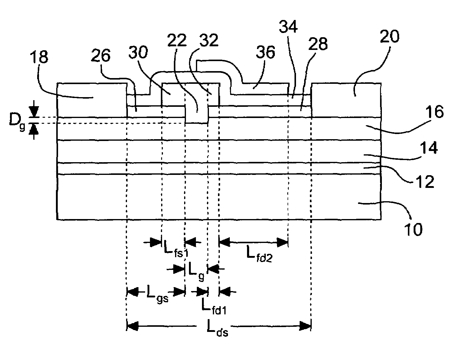
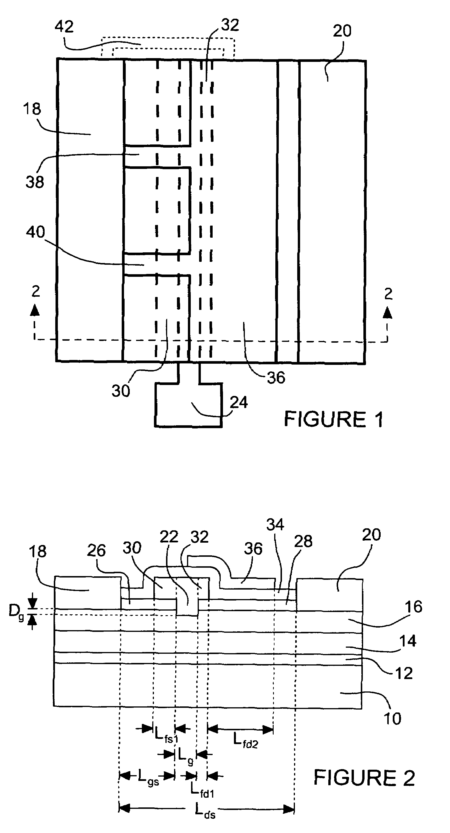
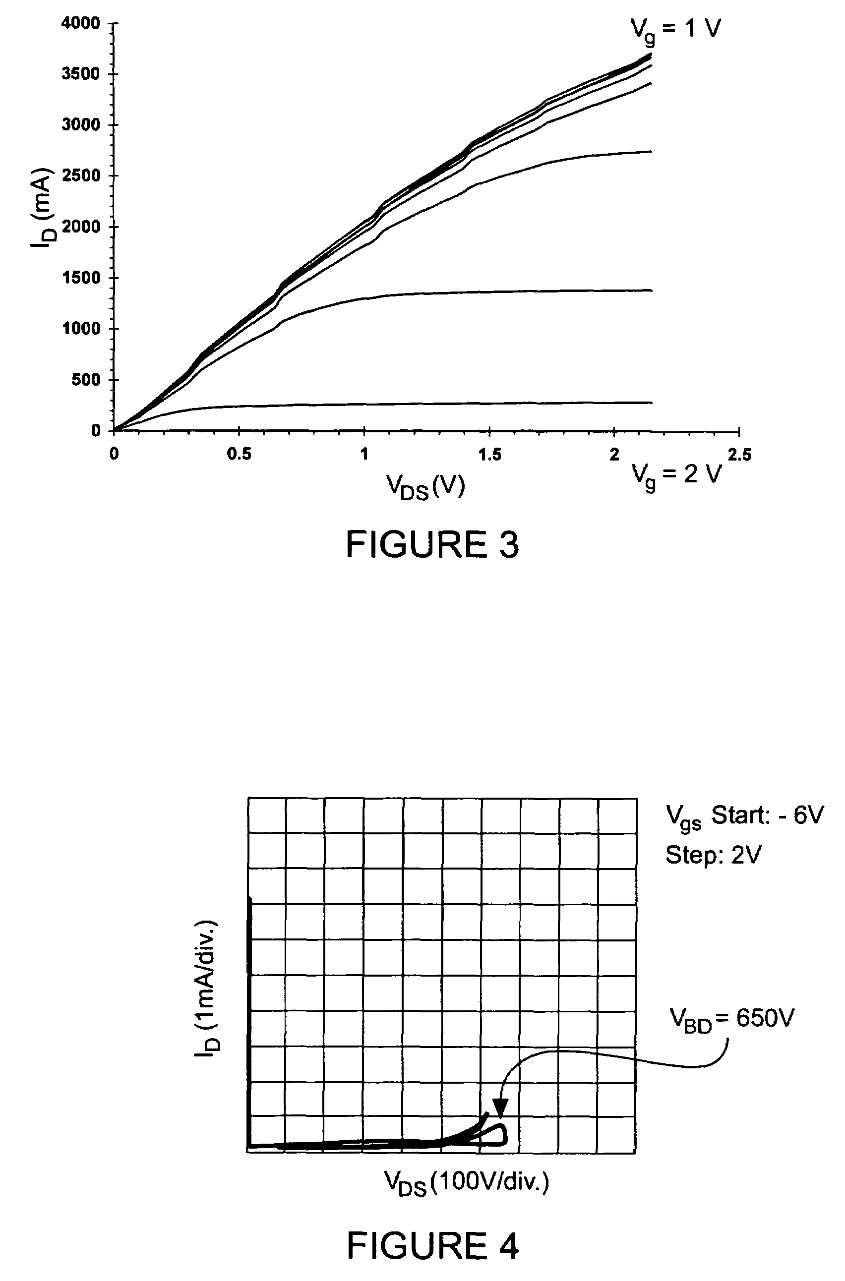
[0040]This invention provides multiple field plate transistors that exhibit increased breakdown voltage and improved power performance, characteristics that are particularly advantageous for power switching applications. In some embodiments, for example, the invention provides transistors with a blocking voltage of at least 600 Volts, while supporting a current of at least 2 Amps with an on resistance of no more than 5.0 mΩ-cm2, and at least 3 Amps, with an on resistance of no more than 5.3 mΩ-cm2; and with a blocking voltage of at least 900 Volts while supporting a current of at least 2 Amps, with an on resistance of no more than 6.6 mΩ-cm2, and at least 3 Amps, with an on resistance of no more than 7.0 mΩ-cm2.

[0041]Embodiments of the present invention may be particularly well suited for use in nitride-based devices such as Group III-nitride based HEMTs. As used herein, the term “Group III nitride” refers to those semiconducting compounds formed between nitrogen and the elements in...


PUM


Abstract

A multiple field plate transistor includes an active region, with a source, a drain, and a gate. A first spacer layer is over the active region between the source and the gate and a second spacer layer over the active region between the drain and the gate. A first field plate on the first spacer layer is connected to the gate. A second field plate on the second spacer layer is connected to the gate. A third spacer layer is on the first spacer layer, the second spacer layer, the first field plate, the gate, and the second field plate, with a third field plate on the third spacer layer and connected to the source. The transistor exhibits a blocking voltage of at least 600 Volts while supporting a current of at least 2 Amps with an on resistance of no more than 5.0 mΩ-cm2, of at least 600 Volts while supporting a current of at least 3 Amps with an on resistance of no more than 5.3 mΩ-cm2, of at least 900 Volts while supporting a current of at least 2 Amps with an on resistance of no more than 6.6 mΩ-cm2, or a blocking voltage of at least 900 Volts while supporting a current of at least 3 Amps with an on resistance of no more than 7.0 mΩ-cm2.

Description

GOVERNMENT RIGHTS[0001]The United States Government has rights in this invention pursuant to contract No. N00014-05-C-0226, awarded by the Office of Naval Research.BACKGROUND OF THE INVENTION[0002]This invention relates to semiconductors, and particularly to transistors for power switching that utilize field plates.[0003]Power semiconductor devices are used as switches or rectifiers in power electronic circuits, such as switch mode power supplies. Common power devices include the power diode, thyristor, power MOSFET and IGBT (insulated gate bipolar transistor). A power diode or MOSFET, for example, operates on principles similar to those of its low power counterparts, but is able to carry a larger amount of current and typically can support a larger reverse-bias voltage in the off state.[0004]Structural changes are often made in power devices to accommodate the higher current density, higher power dissipation and / or higher reverse breakdown voltage required. The vast majority of dis...

Claims


Application Information

Patent Timeline
Patent Type & Authority Patents(United States)
IPC IPC(8): H01L29/93
CPCH01L29/7786H01L29/66462H01L29/404H01L29/2003H01L29/7787
Inventor WU, YIFENGPARIKH, PRIMITMISHRA, UMESH
Owner CREE INC
Why Eureka
Try Eureka