
Nonvolatile memory and semiconductor device including nonvolatile memory

a non-volatile memory, semiconductor technology, applied in static storage, digital storage, instruments, etc., can solve the problems of limited use with short communication distance, power that is necessary for driving, and battery depletion, so as to reduce current consumption and reduce power consumption , the effect of wide communication rang

Inactive Publication Date: 2010-04-06
SEMICON ENERGY LAB CO LTD
View PDF7 Cites 2 Cited by
  • Summary
  • Abstract
  • Description
  • Claims
  • Application Information

AI Technical Summary

Benefits of technology

The present invention aims to provide a nonvolatile memory with reduced power consumption. The invention proposes a structure that reduces the current consumption of writing to the memory by using a resistance element in the writing circuit. The resistance element is placed in a pathway of the current that is necessary for writing. The invention also proposes a structure that reduces the current consumption of reading by using a resistance element in the reading circuit. The nonvolatile memory includes a memory element that has a low resistance state and a high resistance state, and a writing circuit, a resistance element, a voltage source input terminal, a bit line driver circuit, a word line driver circuit, and a transistor. The memory element can transition from a high resistance state to a low resistance state by supplying a potential from the voltage source input terminal. The resistance element is placed in a pathway of the current that is necessary for writing, and the transistor is connected to the memory element through a bit line and the resistance element is placed in a pathway of the current that is necessary for writing. The invention proposes a structure that reduces the current consumption of writing and reading, and provides a nonvolatile memory with a long battery life.

Problems solved by technology

With the active-type wireless tag, there is a problem that the battery is depleted over time depending on the intensity of electric wave necessary for communication, and ultimately, power that is necessary for driving cannot be obtained.
Further, with the passive-type wireless tag, there is a problem that it is limited to uses with short communication distance.
Further, writing to a nonvolatile memory is an operation with large power consumption, since a high voltage or high current is usually necessary.
In this manner, when a nonvolatile memory with large power consumption is mounted to a wireless tag, problems in each type of wireless tag become more pronounced.

Method used


Image

  • Nonvolatile memory and semiconductor device including nonvolatile memory
  • Nonvolatile memory and semiconductor device including nonvolatile memory
  • Nonvolatile memory and semiconductor device including nonvolatile memory

Examples


embodiment mode 1

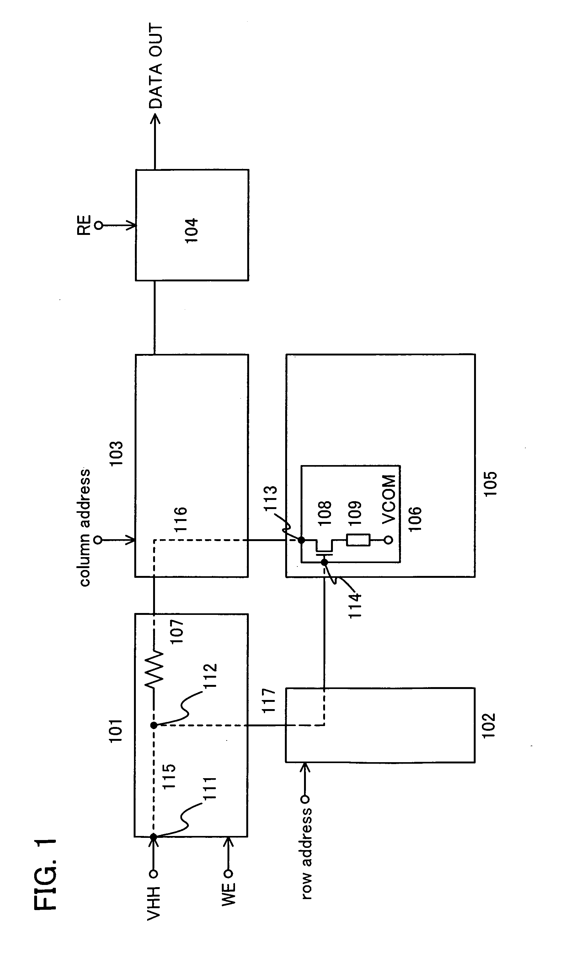
[0048]A structural example of a nonvolatile memory of the present invention is described with reference to the block diagram in FIG. 1.

[0049]The nonvolatile memory shown in FIG. 1 has a writing circuit 101, a word line driver circuit 102, a bit line driver circuit 103, a reading circuit 104, and a memory cell array 105 including a plurality of memory cells 106. Each memory cell 106 has a transistor 108 and a memory element 109.

[0050]A column address is input to the bit line driver circuit 103, and a bit line of a column that the address specifies is connected to the writing circuit 101 or the reading circuit 104. A row address is input to the word line driver circuit 102, and a word line of a row that the address specifies is connected to the writing circuit 101 or a predetermined power source line. A reading control signal RE is input to the reading circuit and a data signal DATA OUT is generated based on a state of the memory element 109 included in the memory cell 106 that is sel...

embodiment mode 2

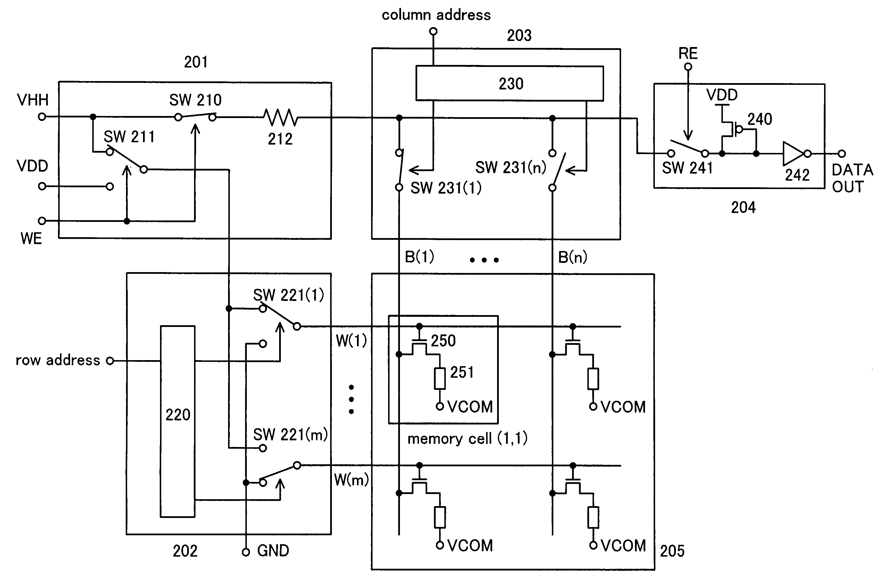
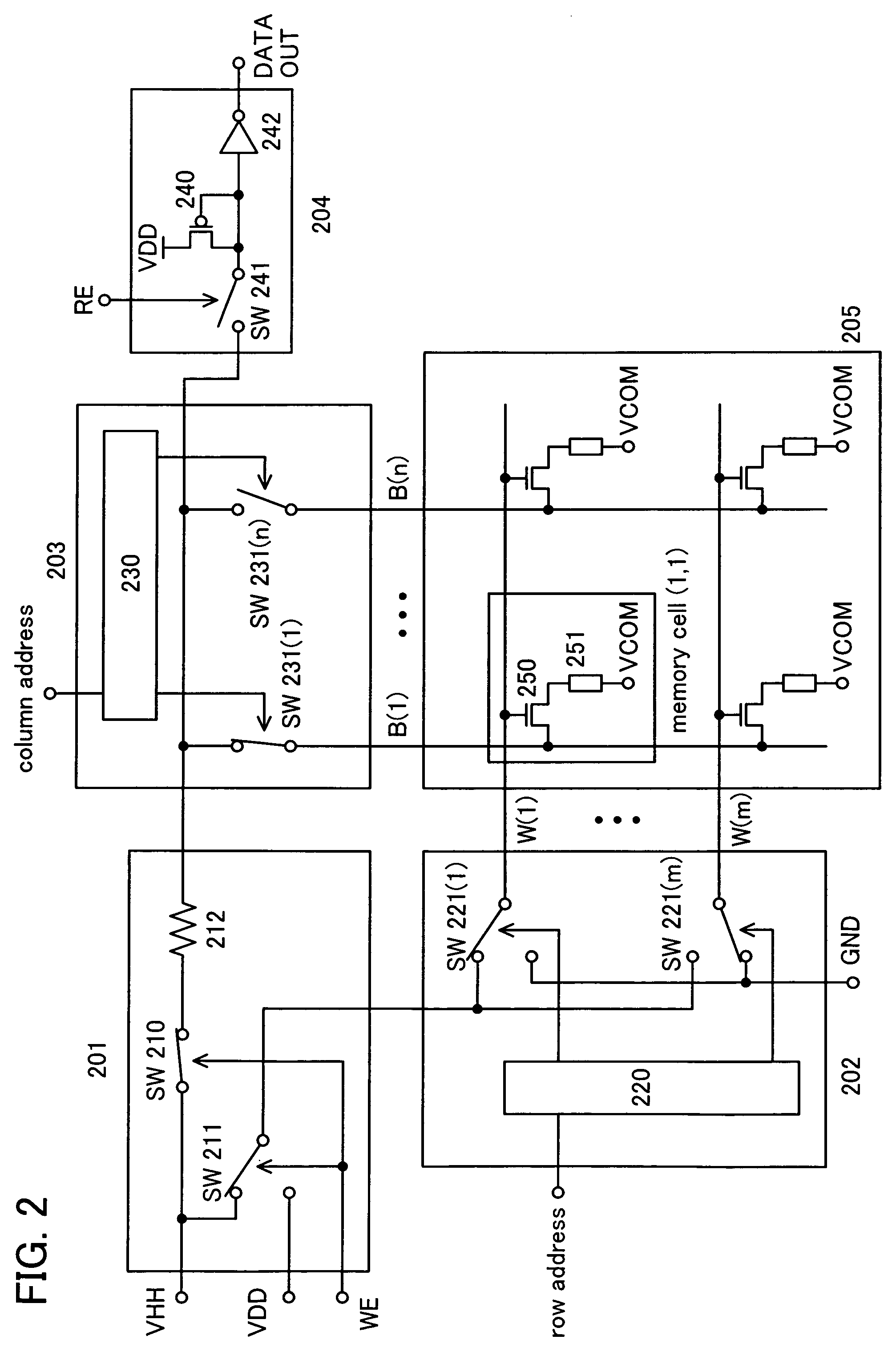
[0068]In this embodiment mode, a structural example of a nonvolatile memory of the present invention is described using FIG. 2.

[0069]The nonvolatile memory shown in FIG. 2 has a writing circuit 201, a word line driver circuit 202, a bit line driver circuit 203, a reading circuit 204, and a memory cell array 205 including memory cells that are arranged in row m and column n.

[0070]The bit line driver circuit 203 includes a column decoder 230 and switches 231(1) to 231(n), and a column address is input thereto. In addition, the bit line driver circuit 203 is connected to the memory cell array 205 by an n number of bit lines B(1) to B(n). The bit line driver circuit 203 turns on a switch 231(k) of a column that is specified by the column address (column k), and connects a bit line B(k) to the writing circuit 201 or the reading circuit 204.

[0071]The word line driver circuit 202 includes a row decoder 220 and switches 221(1) to 221(m), and a row address is input thereto. In addition, the ...

embodiment mode 3

[0089]In this embodiment mode, a structural example of a nonvolatile memory of the present invention is described with reference to FIG. 3.

[0090]The nonvolatile memory shown in FIG. 3 includes a writing circuit 301, a word line driver circuit 302, a bit line driver circuit 303, and a memory cell array 305 including memory cells that are arranged in row m and column n. Note that a reading circuit is included in the bit line driver circuit 303.

[0091]The bit line driver circuit 303 includes a column decoder 330, switches 331(1) to 331(n), switches 332(1) to 332(n), resistance elements 333(1) to 333(n) each composed of a diode-connected transistor, and reading circuits 304(1) to 304(n). A column address is input to the bit line driver circuit 303. In addition, the bit line driver circuit 303 is connected to the memory cell array 305 by an n number of bit lines B(1) to B(n). The bit line driver circuit 303 turns on a switch 331(k) and a switch 332(k) of a column (column k) that is specif...


PUM


Abstract

An object is to provide a nonvolatile memory with reduced power consumption. The nonvolatile memory includes a memory element that has a low resistance state and a high resistance state, a writing circuit, a resistance element, a voltage source input terminal that inputs a writing voltage to the writing circuit, a bit line driver circuit that selects whether the memory element is connected to the writing circuit, and a word line driver circuit that selects whether or not writing is done in the memory element. With such as structure, power consumption during writing can be reduced, and a nonvolatile memory with low power consumption can be realized. Further, with such a nonvolatile memory, an active type wireless tag with a long lifetime of a battery or a passive type wireless tag with a wide communication range in which writing to a memory is possible, can be realized.

Description

BACKGROUND OF THE INVENTION[0001]1. Field of the Invention[0002]The present invention relates to a nonvolatile memory and a semiconductor device including the nonvolatile memory.[0003]2. Description of the Related Art[0004]A memory element composing a nonvolatile memory has a low resistance state and a high resistance state. A memory element is called an anti-fuse type if a resistance is high in an initial state, and it is called a fuse type if the resistance is low in the initial state.[0005]These nonvolatile memories are effective when they are mounted to tags that perform wireless communication (also called “RFID tag,”“wireless tag,” or the like), because they do not need power sources when holding data. In particular, a write-once memory has received attention as a memory with high security, because it cannot be erased once it is written in. Note that wireless tags can be largely classified into two types: an active-type incorporated with a power source (for example, a battery) ...

Claims


Application Information

Patent Timeline
Patent Type & Authority Patents(United States)
IPC IPC(8): G11C5/14
CPCG11C17/165G11C17/16
Inventor KATO, KIYOSHI
Owner SEMICON ENERGY LAB CO LTD
Learn More