Silicon modulator offset tuning arrangement

a technology of modulator and tuning component, applied in the direction of optical waveguide light guide, instruments, optics, etc., can solve the problem of not being able to use lithium niobate-based optical devices in such situations, and achieve the effect of simplifying the overall structure and greatly reducing the optical loss between the modulator and the tuning componen

Active Publication Date: 2010-04-13
CISCO TECH INC
View PDF22 Cites 9 Cited by
  • Summary
  • Abstract
  • Description
  • Claims
  • Application Information

AI Technical Summary

Benefits of technology

[0013]It is a significant advantage of the present invention that the utilization of thermal tuning sections and modulating sections of the same structure (e.g., the SISCAP geometry), the overall structure is simplified, the transition region between the modulator and tuning component is reduced and the optical loss between the modulator and the tuning component is greatly reduced over the prior art.

Problems solved by technology

Clearly, the use of lithium niobate-based optical devices in such a situation is not an option.

Method used


Image

  • Silicon modulator offset tuning arrangement
  • Silicon modulator offset tuning arrangement
  • Silicon modulator offset tuning arrangement

Examples


Embodiment Construction

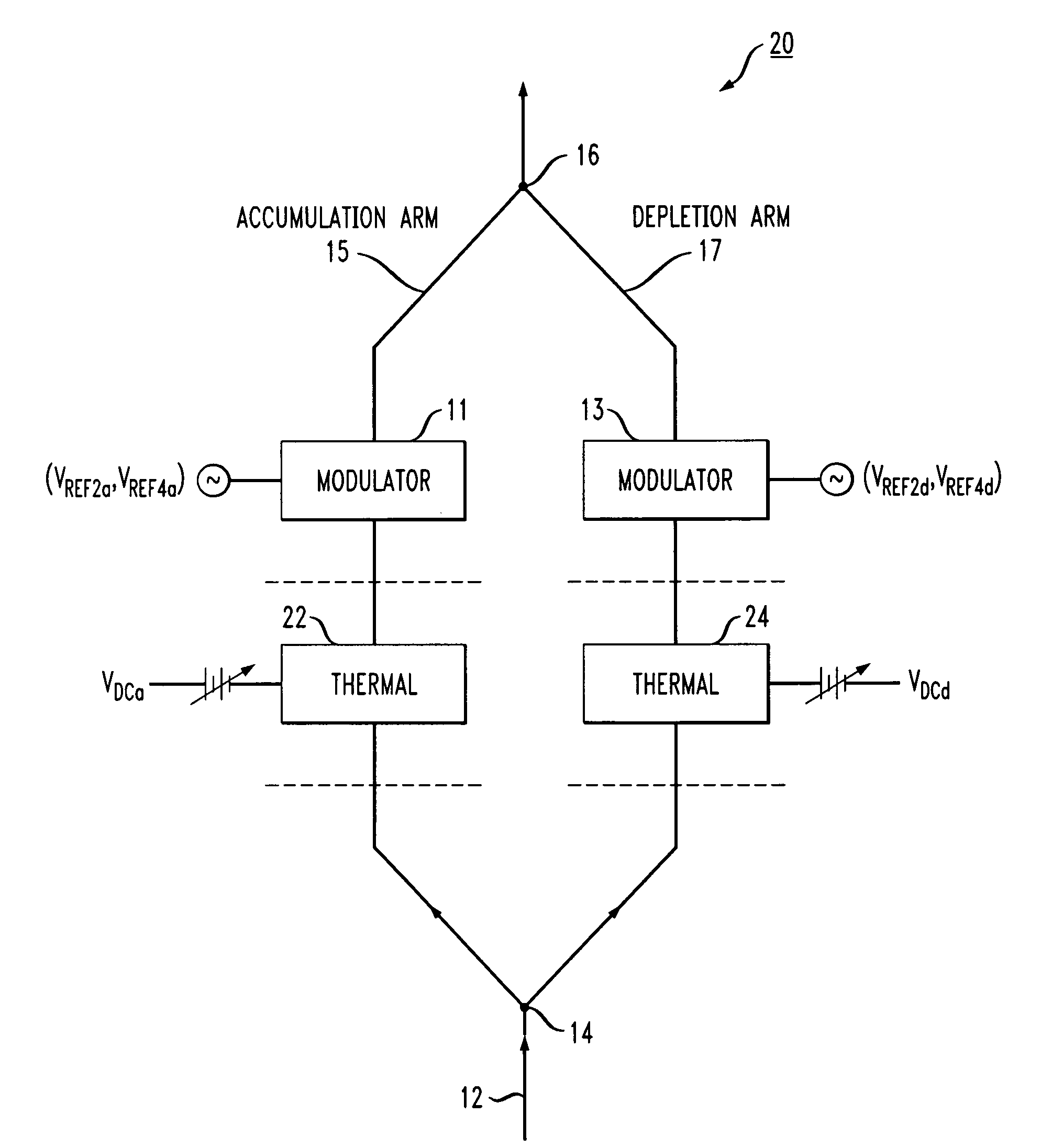
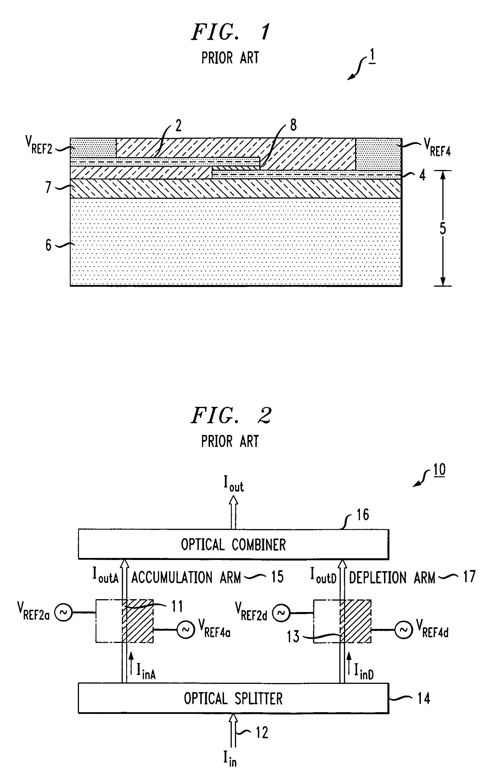
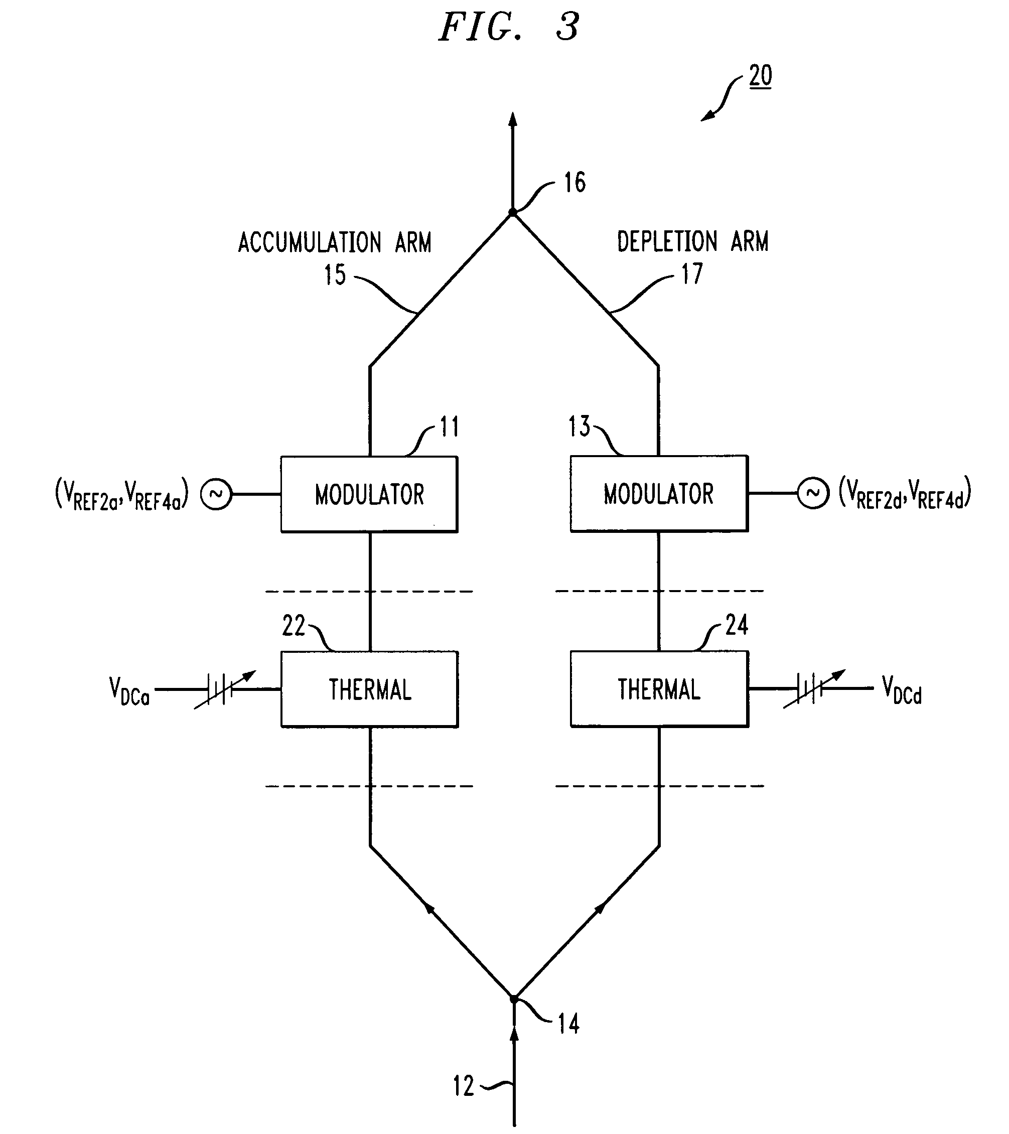
[0026]Prior to describing the utilization of both free carrier modulation and thermal offset control for an SOI-based optical modulator, it is considered helpful to provide an understanding of the operation of a prior art modulator in greater detail. FIG. 2 is a simplified block diagram of an exemplary prior art Mach Zehnder interferometer 10 showing the individual arms of the design, denoted as accumulation arm 15 and depletion arm 17, where interferometer 10 is based upon the prior art structure discussed above in association with FIG. 1. Each arm of interferometer 10 contains a free-carrier-based phase modulator device, controlled by AC modulating signals applied SOI layer 4 and doped silicon layer 2 in the manner described above. The signals applied to each arm operate independent, shown in FIG. 2 as signals VREF2a and VREF4a used to control accumulation arm 15, and signals VREF2d and VREF4d used to control modulation within depletion arm 17. In one embodiment, SOI layer 4 may b...


PUM

PropertyMeasurementUnit
refractive indexaaaaaaaaaa
temperatureaaaaaaaaaa
areaaaaaaaaaaa

Abstract

A silicon-based optical modulator structure includes one or more separate localized heating elements for changing the refractive index of an associated portion of the structure and thereby providing corrective adjustments to address unwanted variations in device performance. Heating is provided by thermo-optic devices such as, for example, silicon-based resistors, silicide resistors, forward-biased PN junctions, and the like, where any of these structures may easily be incorporated with a silicon-based optical modulator. The application of a DC voltage to any of these structures will generate heat, which hen transfers into the waveguiding area. The increase in local temperature of the waveguiding area will, in turn, increase the refractive index of the waveguiding in the area. Control of the applied DC voltage results in controlling the refractive index.

Description

CROSS-REFERENCE TO RELATED APPLICATION[0001]This application is a continuation-in-part of U.S. Ser. No. 11 / 810,591, filed Jun. 6, 2007, now U.S. Pat. No. 7,447,395 which claims the benefit of U.S. Provisional Application No. 60 / 813,913, filed Jun. 15, 2006, and U.S. Provisional Application No. 60 / 928,386, filed May 9, 2007.TECHNICAL FIELD[0002]The present invention relates to an arrangement for providing independent control of modulation characteristics (phase and amplitude) and offset (bias) in an SOI-based optical modulator utilizing thermo-optic adjustment techniques.BACKGROUND OF THE INVENTION[0003]For many years, external optical modulators have been made out of electro-optic material, such as lithium niobate. Optical waveguides are formed within the electro-optic material, with metal contact regions disposed on the surface of each waveguide arm. The application of a voltage to a metal contact will modify the refractive index of the waveguide region underneath the contact, thus...

Claims


Application Information

Patent Timeline
Patent Type & Authority Patents(United States)
IPC IPC(8): G02B6/12G02F1/295
CPCG02F1/225G02F1/025G02F1/0147G02F2201/126
Inventor WEBSTER, MARKPATEL, VIPULKUMARGOTHOSKAR, PRAKASH
Owner CISCO TECH INC
Why Eureka
Try Eureka