Reversible leadless package and methods of making and using same

a leadless, semiconductor technology, applied in the direction of semiconductor devices, semiconductor/solid-state device details, electrical apparatus, etc., can solve the problems of unsalvageable entire package, unsalvageable entire package, and complicated assembly of the package with stacked dies

Active Publication Date: 2010-05-04
UNISEM M BERHAD
View PDF18 Cites 36 Cited by
  • Summary
  • Abstract
  • Description
  • Claims
  • Application Information

AI Technical Summary

Problems solved by technology

This solution, however, has its drawbacks.
First, a package with stacked dies introduces complexity in the assembly of the package due at least in part to the increased number of electrical connections within the package and the need for an insulative layer / interposer to be disposed between the dies.
If any defects occur during the assembly of the package, the entire package, including all chips within the stack, is unsalvageable.
Finally, stacking two or more dies in a single package increases the thickness of the encapsulated package and creates issues for power management and thermal drain.

Method used


Image

  • Reversible leadless package and methods of making and using same
  • Reversible leadless package and methods of making and using same
  • Reversible leadless package and methods of making and using same

Examples


Embodiment Construction

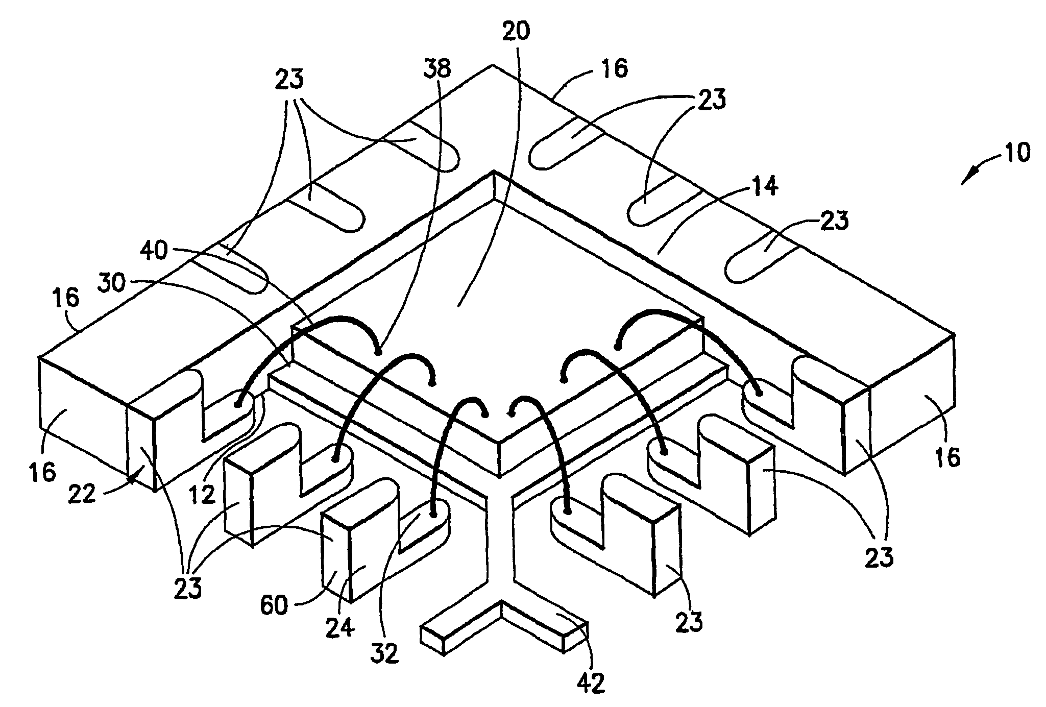
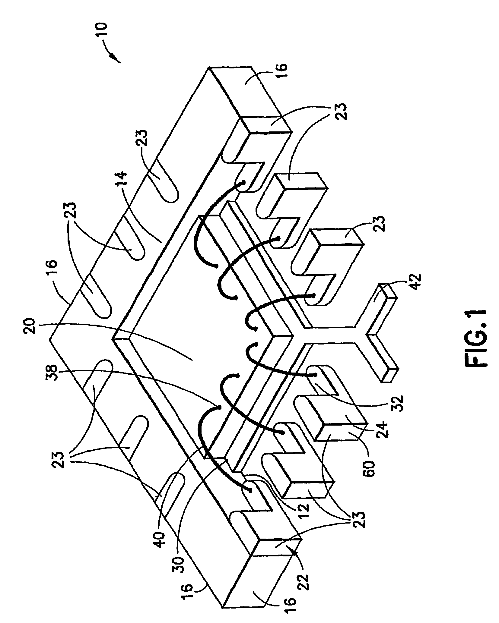
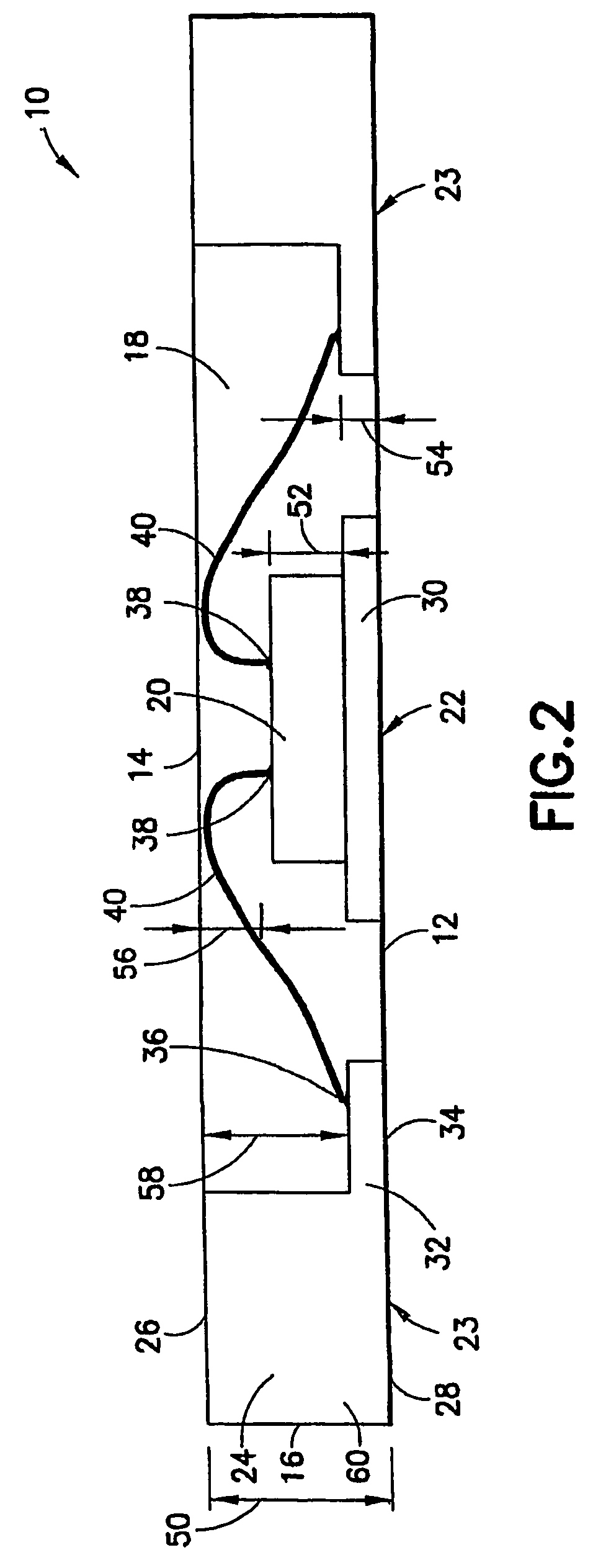
[0034]Referring to FIGS. 1 and 2, a quad, no-lead, wirebonded semiconductor device package 10 is shown. The semiconductor device package 10 has a bottom package face 12, a top package face 14 opposite the bottom package face 12, and package side faces 16 extending between the bottom and top package faces 12, 14. The various package faces are formed in part by a molding compound 18, which covers a semiconductor device (die) 20 and portions of an electrically conductive lead frame 22. The electrically conductive lead frame 22 includes a plurality of leads 23. Each of the leads 23 includes a post 24 disposed at a perimeter of the package. Each of the posts 24 has a first contact surface 26 disposed at the top package face 14 and a second contact surface 28 disposed at the bottom package face 12. The die 20 is attached to a die support pad 30 positioned in a central region formed by the plurality of posts 24. Each lead 23 also includes a post extension 32, having a contact surface 34 di...


PUM


Abstract

A semiconductor device package includes an electrically conductive lead frame having a plurality of posts disposed at a perimeter of the package. Each of the posts has a first contact surface disposed at the first package face and a second contact surface disposed at the second package face. The lead frame also includes a plurality of post extensions disposed at the second package face. Each of the post extensions includes a bond site formed on a surface of the post extension opposite the second package face. At least one I / O pad on the semiconductor device is electrically connected to the post extension at the bond site using wirebonding, tape automated bonding, or flip-chip methods. The package can be assembled using a lead frame having pre-formed leads, with or without taping, or using partially etched lead frames. A stack of the semiconductor device packages may be formed.

Description

CROSS-REFERENCE TO RELATED APPLICATIONS[0001]This application claims the benefit of U.S. Provisional Patent Application No. 60 / 497,829, filed Aug. 26, 2003, which is incorporated by reference herein in its entirety.BACKGROUND OF THE INVENTION[0002]1. Field of the Invention[0003]This invention relates to semiconductor device packages. More particularly, this invention relates to reversible leadless semiconductor device packages and methods for manufacturing reversible leadless semiconductor device packages.[0004]2. Description of the Related Art[0005]In lead frame based semiconductor device packages, electrical signals are transmitted between at least one semiconductor device (die) and external circuitry, such as a printed circuit board, by an electrically conductive lead frame. The lead frame includes a plurality of leads, each having an inner lead end and an opposing outer lead end. The inner lead end is electrically connected to an input / output (I / O) pad on the die, and the outer ...

Claims


Application Information

Patent Timeline
Patent Type & Authority Patents(United States)
IPC IPC(8): H01L23/495H01L23/28H01LH01L21/44H01L21/48H01L23/31H01L25/10
CPCH01L21/4832H01L21/561H01L21/568H01L23/3107H01L23/3128H01L23/49548H01L24/97H01L25/105H01L2224/32257H01L2224/16245H01L2225/1058H01L2225/1029H01L2924/01006H01L2924/01005H01L24/48H01L2924/18161H01L2924/15311H01L2924/01082H01L2924/01079H01L2221/68377H01L2224/16H01L2224/2919H01L2224/48091H01L2224/48247H01L2224/84439H01L2224/92247H01L2224/97H01L2924/01013H01L2924/01015H01L2924/01027H01L2924/01029H01L2924/01033H01L2924/01078H01L2224/85H01L2924/00014H01L2924/0665H01L2224/83H01L2224/81H01L2924/181H01L2224/05573H01L2224/05568H01L2224/45144H01L24/45H01L2924/00012H01L2224/05599H01L2224/45015H01L2924/207H01L2224/37099H01L23/495
Inventor ISLAM, SHAFIDULSAN ANTONIO, ROMARICO S.
Owner UNISEM M BERHAD
Why Eureka
Try Eureka