
Audio power amplifier package

a power amplifier and audio technology, applied in the field of packages, can solve the problems of serious affecting the operation of the power amplifier and the band-gap reference circuit, and achieve the effect of improving the power supply rejection ratio (psrr), and improving the total harmonic distortion plus noise (thd+n)

Inactive Publication Date: 2010-05-04
HIMAX ANALOGIC INC
View PDF2 Cites 0 Cited by
  • Summary
  • Abstract
  • Description
  • Claims
  • Application Information

AI Technical Summary

Benefits of technology

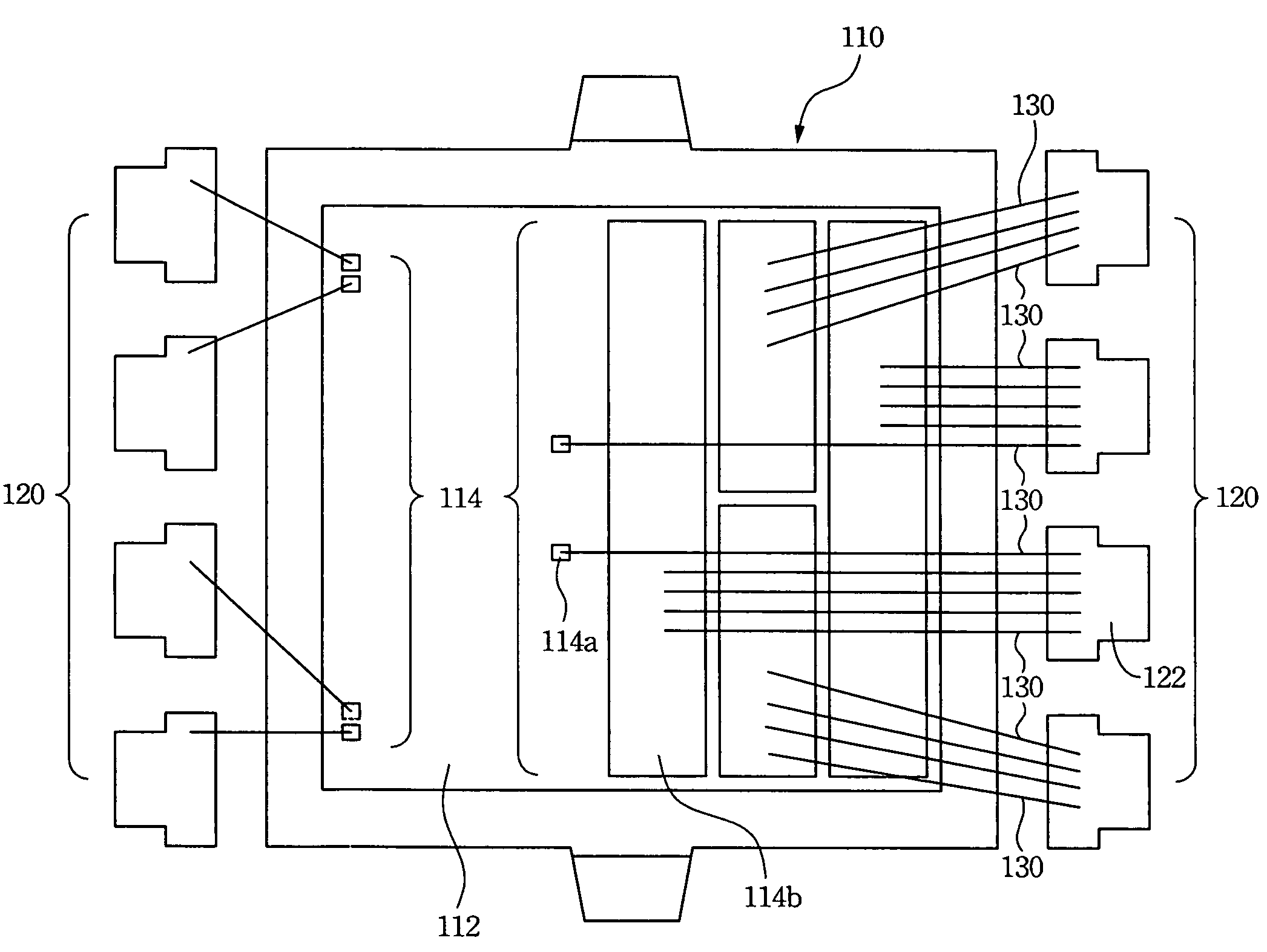
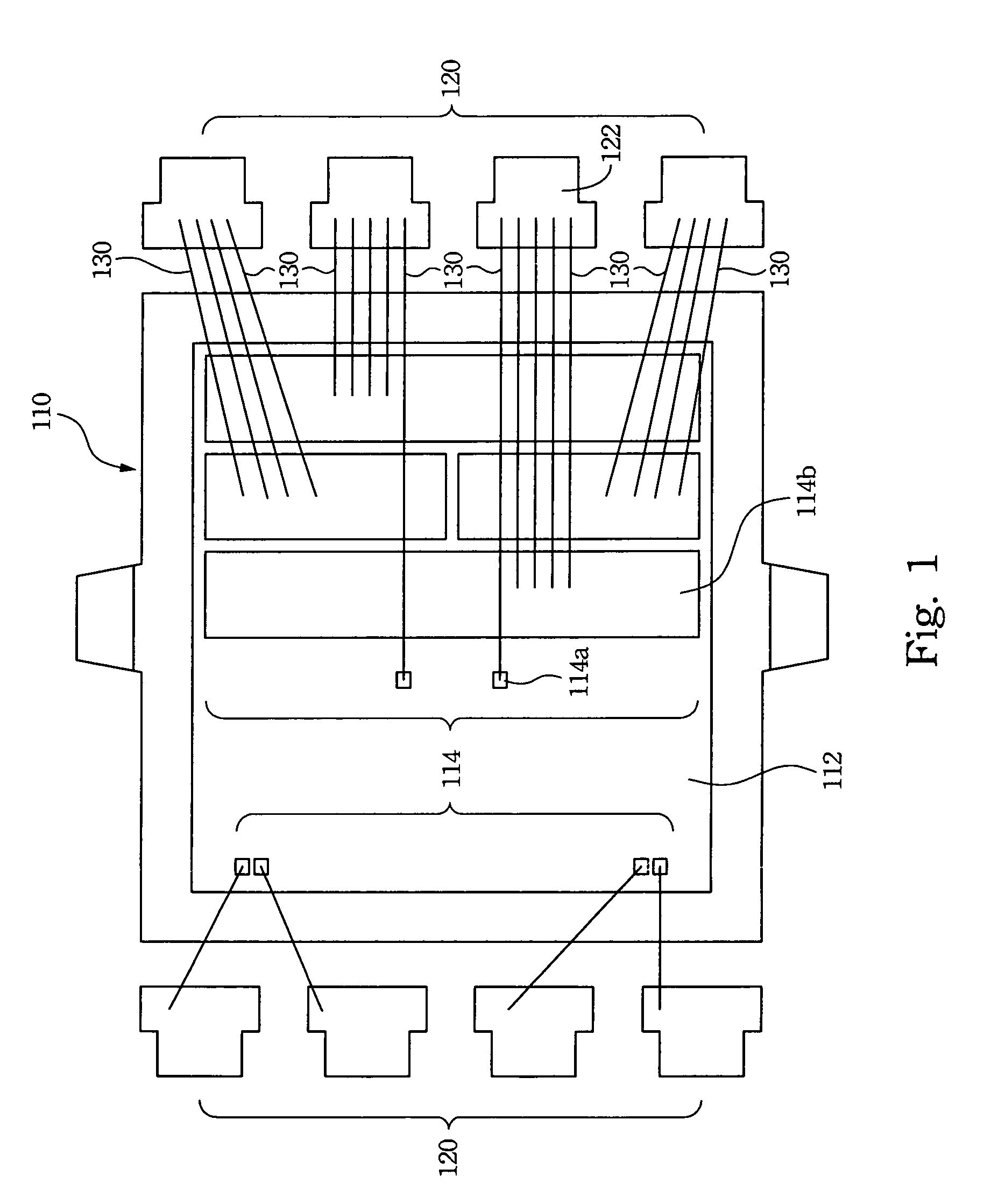
"The present invention provides an audio power amplifier package that can improve power supply rejection ratio (PSRR) and reduce interference and power noise. The package includes a substrate, pads, leads, and bonding wires. The pads include a first non-signal pad and a second non-signal pad, while the leads include a non-signal lead. The bonding wires connect the non-signal lead to the first non-signal pad and the second non-signal pad, respectively. The technical effects of the invention include improved audio power amplifier performance and reduced interference and power noise."

Problems solved by technology

Thus, the switches which need high switching power usually produce some interference and power noise to seriously affect the operational amplifiers and band-gap reference circuits which need pure power.

Method used


Image

  • Audio power amplifier package
  • Audio power amplifier package

Examples


Embodiment Construction

[0012]In the following detailed description, the embodiment of the present invention has been shown and described. As will be realized, the invention is capable of modification in various obvious respects, all without departing from the invention. Accordingly, the drawings and description are to be regarded as illustrative in nature, and not restrictive.

[0013]The embodiment of the present invention discloses an audio power amplifier package, which includes a non-signal lead, two non-signal pads and a plurality of bonding wires. The bonding wires connect the non-signal lead to both of the non-signal pads respectively, such that signals can be separately transmitted from the non-signal lead to both of the non-signal pads through the bonding wires. Therefore, the interference and power noise can be avoided during the operation of the audio power amplifier.

[0014]FIG. 1 is a top view of an audio power amplifier package according to one embodiment of the present invention. The audio power...


PUM


Abstract

An audio power amplifier package includes a non-signal lead, a first non-signal pad, a second non-signal pad and a plurality of bonding wires. The first non-signal pad and the second non-signal pad are disposed on a substrate. The bonding wires connect the non-signal lead to the first non-signal pad and the second non-signal pad respectively.

Description

BACKGROUND[0001]1. Field of Invention[0002]The present invention relates to a package. More particularly, the present invention relates to an audio power amplifier package.[0003]2. Description of Related Art[0004]Modern electronic products typically enclose a semiconductor chip and a carrier for electrically connecting with the semiconductor chip. At present, there are three major techniques for connecting a chip to a carrier, namely, a wire-bonding process, a flip-chip process and a tape-automated-bonding (TAB) process. If the carrier is a lead frame, the wire-bonding process is often used to connect the chip with the leads on the lead frame.[0005]For a conventional audio power amplifier which is fabricated by using the wire-bonding process, in order to meet the need for package size and die size when designing the audio power amplifier, switches and other circuits, such as operational amplifiers and band-gap reference circuits, in the audio power amplifier have to be powered at on...

Claims


Application Information

Patent Timeline
Patent Type & Authority Patents(United States)
IPC IPC(8): H01L23/12
CPCH01L23/4952H01L24/06H01L24/49H01L2924/01033H01L2924/00014H01L24/48H01L2924/01082H01L2224/85399H01L2224/49175H01L2224/49171H01L2224/49111H01L2224/48247H01L2224/0603H01L2224/05599H01L2223/6611H01L2924/00H01L2224/45099H01L2924/00012H01L2224/05553H01L2224/05554H01L2224/49113H01L2924/10161
Inventor WU, KUO-HUNGLI, PO-YU
Owner HIMAX ANALOGIC INC
Learn More