E/D NMOS reference voltage source with high electric power rejection ratio
A technology with high power supply rejection ratio and reference voltage source, applied in control/regulation systems, regulating electrical variables, instruments, etc. The structure is simple and reasonable, the effect of improving the power supply rejection ratio and simplifying the process
- Summary
- Abstract
- Description
- Claims
- Application Information
AI Technical Summary
Problems solved by technology
Method used
Image
Examples
Embodiment Construction
[0021] The specific implementation manners of the present invention are not limited to the following description, and are now further described in conjunction with the accompanying drawings.
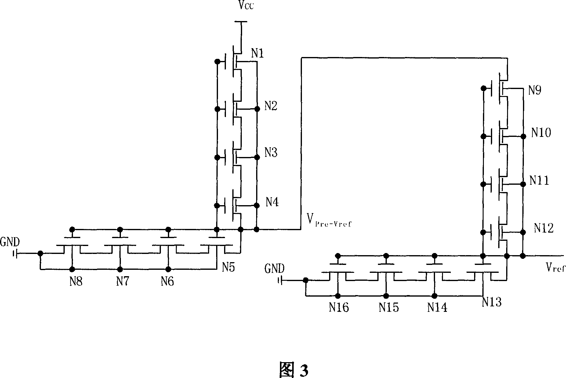
[0022] The circuit diagram of the E / DNMOS reference voltage source embodied in the present invention is shown in FIG. 3 . It is composed of an E / DNMOS pre-reference source circuit and a reference source circuit. The specific structure, connection relationship and function relationship are the same as the content of the invention in this specification, and will not be repeated here. It works like this:
[0023] For ease of calculation, the depletion-type NMOS transistors N1, N2, N3, and N4 are regarded as an equivalent NMOS transistor N1 * , whose threshold voltage is N TD , the channel width is W N1 , the channel length is L N1 ;Similarly, the NMOS tube enhanced N5, N6, N7, N8 is regarded as an equivalent NMOS tube N2 * , whose threshold voltage is N T2 , the channel width is W N2...
PUM
 Abstract
Description
Claims
Application Information


