Fin field effect transistor arrangement and method for producing a fin field effect transistor arrangement

a technology of fin field effect transistor and arrangement, which is applied in the direction of transistors, electrical devices, semiconductor devices, etc., can solve the problems of large area requirement for realizing the circuit on a silicon chip, cost pressure in semiconductor technology, and loss of valuable silicon area, etc., and achieve good quality and reproducibility. the effect of

Inactive Publication Date: 2010-05-18
INFINEON TECH AG
View PDF19 Cites 23 Cited by
  • Summary
  • Abstract
  • Description
  • Claims
  • Application Information

AI Technical Summary

Benefits of technology

[0031]In the case of the fin field effect transistor arrangement, the fin of the first fin field effect transistor may have doping material of the p conduction type (e.g., arsenic, phosphorus) and the fin of the second fin field effect transistor may either have doping material of the n conduction type (e.g., aluminum, boron) or be free of doping material (or have only small quantities of intrinsic doping). It is not necessary, therefore, for the channel regions of both fin field effect transistors of the fin field effect transistor arrangement to be doped, rather the advantageous effects of the invention can be achieved even when one of the channel regions is doped and the other is either doped with doping atoms of the opposite conduction type or undoped.
[0032]Therefore, in the case of the fin field effect transistor arrangement, the fin of the first fin field effect transistor may either have doping material of the p conduction type or be free of doping material and the fin of the second fin field effect transistor may have doping material of the n conduction type.
[0033]To express it more generally, the two fin field effect transistors may have different conduction types, in which case the resultant different transistor properties (primarily current driver capabilities) can be compensated for by means of setting different fin heights.
[0034]The fin field effect transistor arrangement of the invention may be set up as a CMOS arrangement, that is to say as an arrangement comprising n-channel fin field effect transistors and p-channel fin field effect transistors, it being possible for the current driver capabilities and other transistor properties to be coordinated with one another by means of adjusting the height of the fin of the two types of transistor. For this purpose, the height of the fin field effect transistor of the p conduction type is generally chosen to be higher than that of the n-fin field effect transistor.
[0035]The height of the fin of the first fin field effect transistor and the height of the fin of the second fin field effect transistor may be adjusted in such a way that the current driver capability of the first fin field effect transistor is substantially equal to the current driver capability of the second fin field effect transistor. An integrated circuit obtained in this way has a good quality and reproducible properties.
[0036]The substrate may be an SOI substrate (silicon-on-insulator). In this case, the fins may be formed in the upper silicon layer of such an SOI substrate. Since the fin height in this case is determined by the thickness of the SOI substrate, in particular of the upper silicon layer of an SOI substrate, an SOI substrate that has different top silicon thicknesses is advantageous.

Problems solved by technology

However, increasing the transistor width of the p-channel transistor in a CMOS circuit has the disadvantage that this enlarges the area requirement for realizing the circuit on a silicon chip.
Valuable silicon area is lost as a result, which is disadvantageous in view of the cost pressure in semiconductor technology.
This is disadvantageous since the necessary chip area for forming the transistors 100, 110 is thereby enlarged.
However, even in fin field effect transistors the problem arises that p-fin field effect transistors have current driver capabilities or generally transistor properties which differ from the current driver capabilities or transistor properties of an n-fin field effect transistor given identical dimensioning.
However, this concept has the disadvantage that the space requirement of the transistor arrangement is increased by means of dividing the fin into a plurality of partial fins, which counteracts the endeavor to increase the integration density.
Consequently, the provision of a plurality of partial fins considerably increases the area requirement.

Method used


Image

  • Fin field effect transistor arrangement and method for producing a fin field effect transistor arrangement
  • Fin field effect transistor arrangement and method for producing a fin field effect transistor arrangement
  • Fin field effect transistor arrangement and method for producing a fin field effect transistor arrangement

Examples


Embodiment Construction

[0098]Identical or similar components in different figures are provided with identical reference numerals.

[0099]The illustrations in the figures are schematic and not to scale.

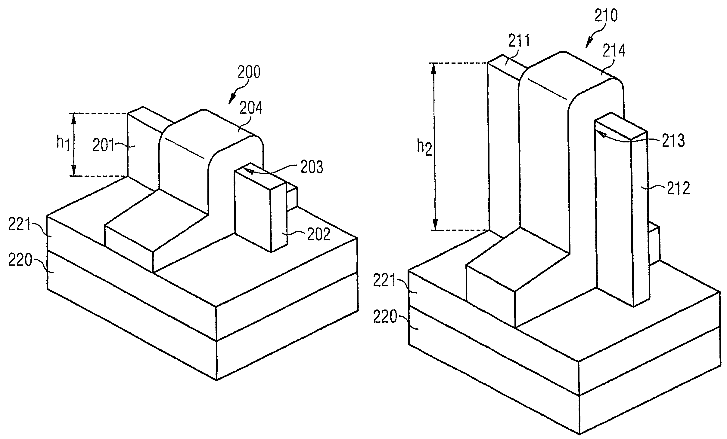
[0100]A description is given below, referring to FIG. 2A, FIG. 2B, of an n-MOS fin field effect transistor 200 and a p-MOS fin field effect transistor 210, which are integrated in a fin field effect transistor arrangement according to the invention and in a common substrate.

[0101]The fin field effect transistor arrangement from FIG. 2A, FIG. 2B, which contains the n-MOS fin field effect transistor 200 and the p-MOS fin field effect transistor 210, has a silicon substrate 220, on which a silicon oxide layer 221 is formed. Although transistors 200, 210 are illustrated separately in FIG. 2A, FIG. 2B, both fin field effect transistors 200, 210 are monolithically integrated in the same substrate 220.

[0102]The n-MOS fin field effect transistor 200 contains a silicon fin having the height h1. A first source / drain reg...


PUM


Abstract

A fin field effect transistor arrangement comprises a substrate and a first fin field effect transistor on and / or in the substrate. The first fin field effect transistor includes a fin in which a channel region is formed between a first source / drain region and a second source / drain region and above which a gate region is formed. A second fin field effect transistor is provided on and / or in the substrate including a fin in which a channel region is formed between a first source / drain region and a second source / drain region and above which a gate region is formed. The second fin field effect transistor is arranged laterally alongside the first fin field effect transistor, wherein a height of the fin of the first fin field effect transistor is greater than a height of the fin of the second fin field effect transistor.

Description

[0001]This application is a continuation of co-pending International Application No. PCT / DE2005 / 000746, filed Apr. 22, 2005, which designated the United States and was not published in English, and which is based on German Application No. 10 2004 020 593.0 filed Apr. 27, 2004, both of which applications are incorporated herein by reference.TECHNICAL FIELD[0002]The invention relates to a fin field effect transistor arrangement and a method for producing a fin field effect transistor arrangement.BACKGROUND[0003]In CMOS technology, circuits are formed that are integrated on a substrate, the circuits having n-channel field effect transistors and p-channel field effect transistors. When the transistors of different conduction types are dimensioned identically, it happens that an n-channel transistor of a CMOS circuit has a different current driver capability than a p-channel transistor of the circuit.[0004]In the case of integrated circuit components in CMOS technology that have n-MOS tr...

Claims


Application Information

Patent Timeline
Patent Type & Authority Patents(United States)
IPC IPC(8): H01L21/84H01L21/8238H01L27/12H01L29/786
CPCH01L21/845H01L27/1211H01L29/78636H01L29/785H01L29/66795
Inventor HOFMANN, FRANZLANDGRAF, ERHARDLUYKEN, RICHARD JOHANNES
Owner INFINEON TECH AG
Why Eureka
Try Eureka