

Semiconductor light-emitting device and manufacturing method thereof
a technology of semiconductors and light-emitting devices, which is applied in the direction of discharge tubes/lamp details, instruments, luminescent screens of discharge tubes, etc., can solve the problems of increasing the total manufacturing cost and the inability of silicon substrates to transmit light, so as to reduce the amount of light directed, the effect of efficient directed ligh
- Summary
- Abstract
- Description
- Claims
- Application Information
AI Technical Summary
Benefits of technology
Problems solved by technology
Method used
Image

Examples
first embodiment
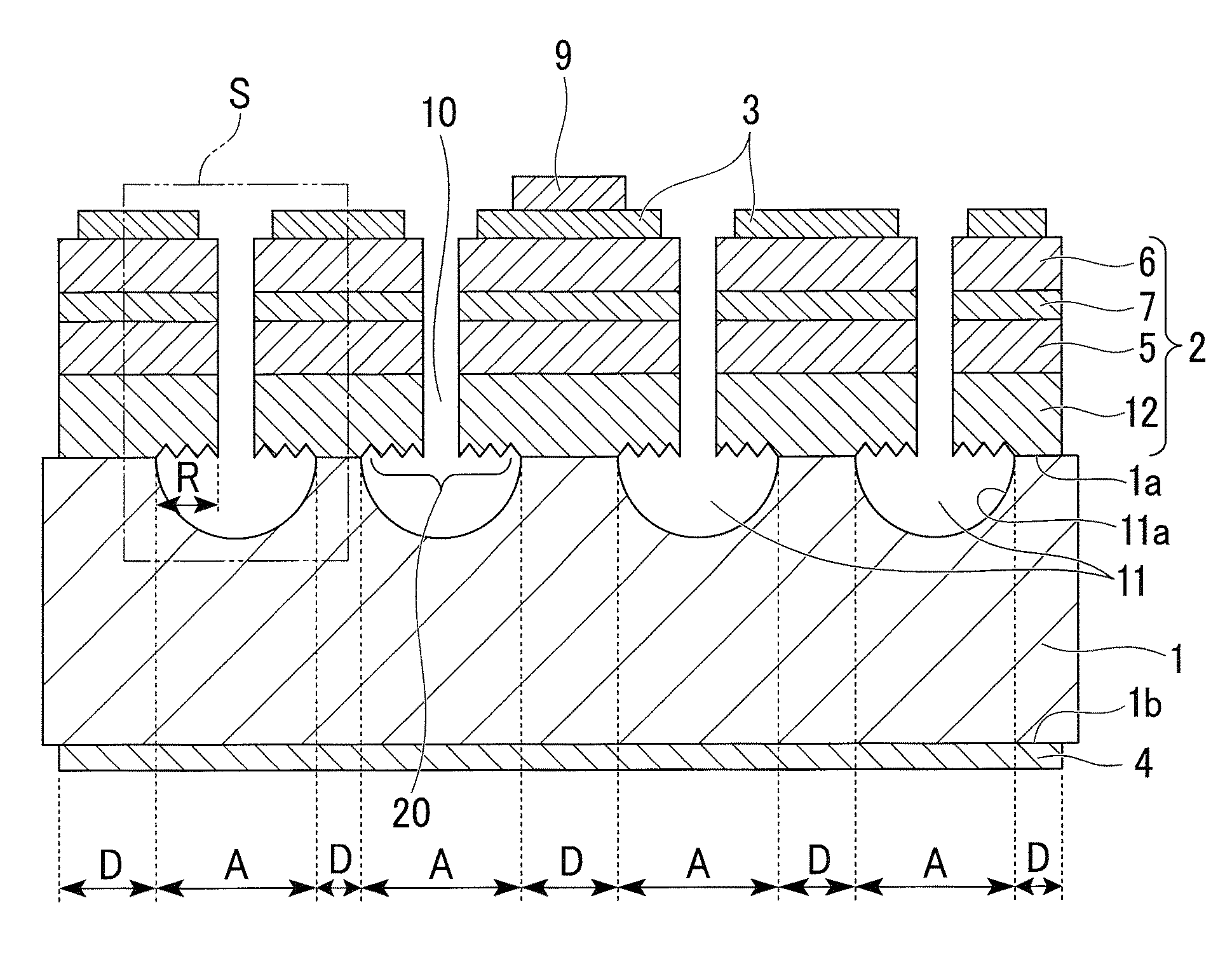
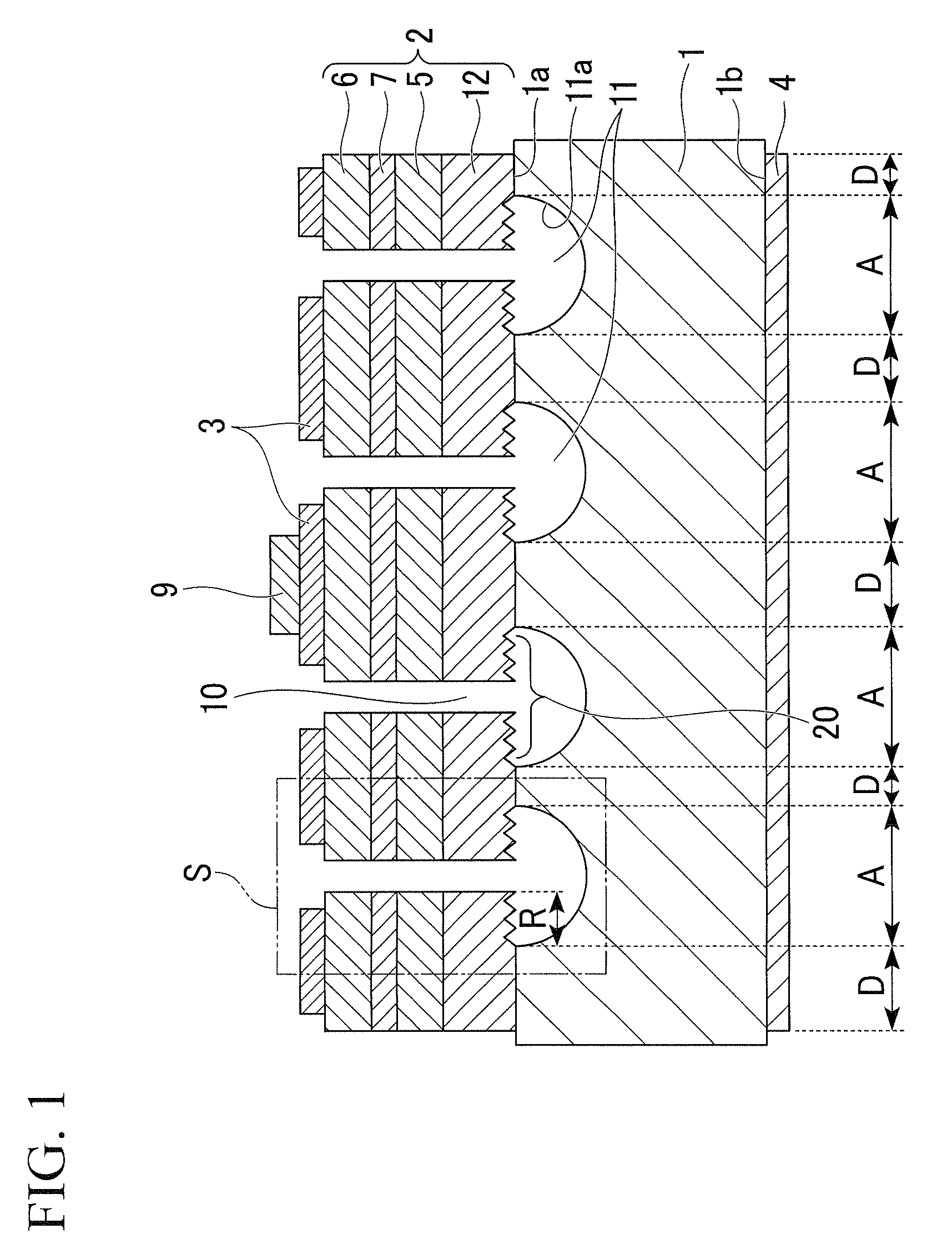
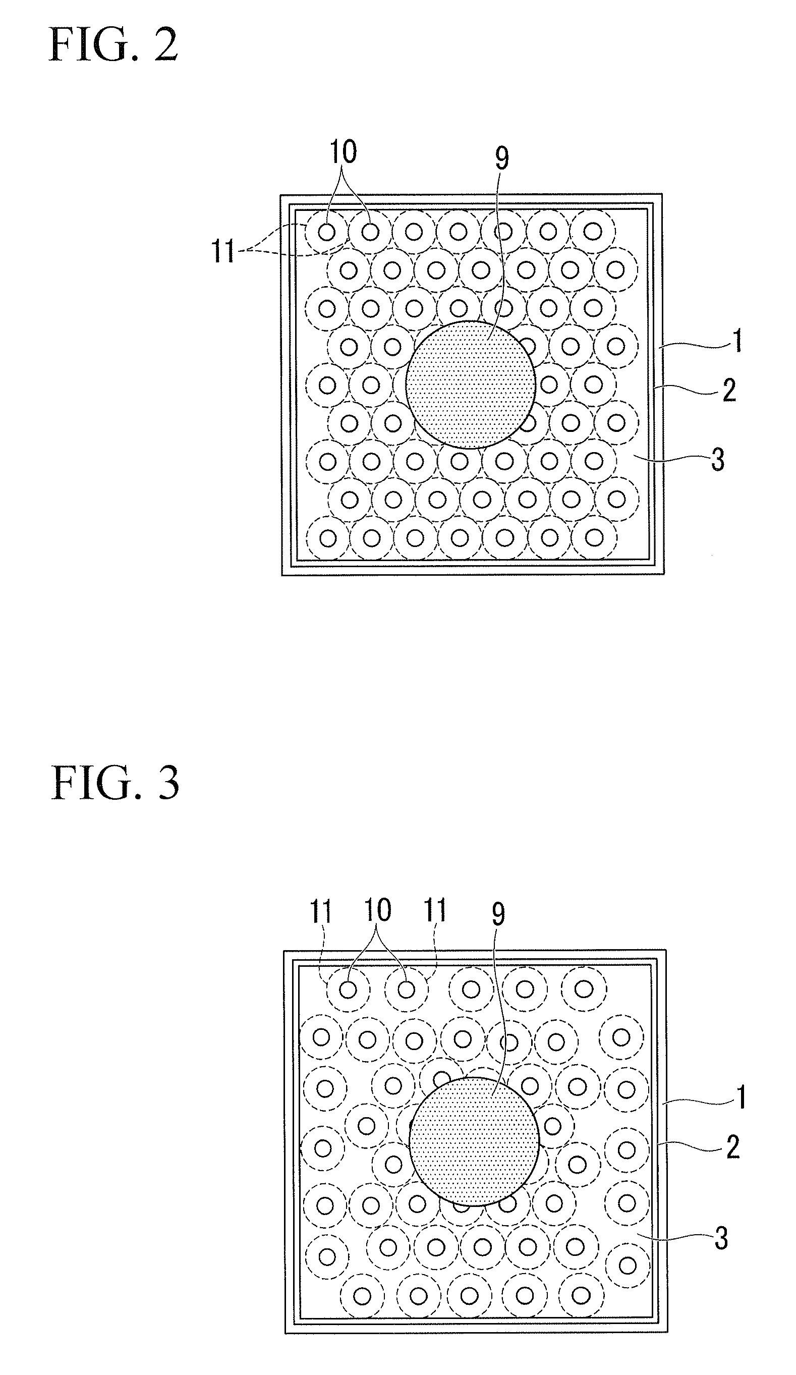
[0061]Below, a first embodiment of the present invention will be explained. FIGS. 2 to 4 are plan views showing the structure of a semiconductor light-emitting device in the present embodiment, when the device is observed from above. FIG. 1 is a diagram showing a sectional structure of the semiconductor light-emitting device along line A-A in FIG. 4. Here, FIGS. 1 to 4 are schematic diagrams for showing the structure in an easily-understandable manner, and the size of each structural element in FIG. 1 does not accurately correspond to the relevant one in FIG. 4.
[0062]In FIG. 1, the present semiconductor light-emitting device has (i) a conductive substrate 1 having a main surface 1a (i.e., one of two main surfaces), and a main surface 1b (i.e., the other main surface), in which hollow parts 11 are formed in the main surface 1a, (ii) an active layer forming part 2 having a light-emitting function, (iii) a first electrode 3, (iv) a second electrode 4, (v) a pad electrode 9, and (vi) ho...
second embodiment
[0138]The structure of a semiconductor light-emitting device as a second embodiment of the present invention will be explained with reference to FIGS. 9A and 9B. FIG. 9A is a diagram showing a sectional structure of the semiconductor light-emitting device of the second embodiment and FIG. 9B is an enlarged view of a part 500 in FIG. 9A. In FIGS. 9A and 9B, parts similar to those in the first embodiment are given identical reference numerals, and explanations thereof are omitted. More specifically, the second embodiment has a structure similar to the first embodiment, except for a part of the conductive substrate 1 and a part where a protective element is formed, immediately under a pad electrode 9. The structure in plan view is similar to those shown in FIGS. 2 to 4 because a protective-element forming area is covered by the pad electrode 9.
[0139]The present embodiment relates to a composite semiconductor device which includes a semiconductor light-emitting device and a protective e...
PUM
 Abstract
Description
Claims
Application Information