Attachment method, attachment apparatus, manufacturing method of semiconductor device, and manufacturing apparatus of semiconductor device
a manufacturing method and semiconductor technology, applied in semiconductor devices, semiconductor/solid-state device details, instruments, etc., can solve the problems of long takt time, high manufacturing cost of semiconductor devices, and inability to electrically connect a plurality of semiconductor integrated circuits formed over an element substrate to a plurality of antennas over a flexible substrate simultaneously, so as to improve pass productivity and reduce the time , the effect of low cos
- Summary
- Abstract
- Description
- Claims
- Application Information
AI Technical Summary
Benefits of technology
Problems solved by technology
Method used
Image

Examples
embodiment mode 1
[0062]A manufacturing method of a semiconductor device of the present invention is described. The description is given with reference to FIGS. 1A to 10.
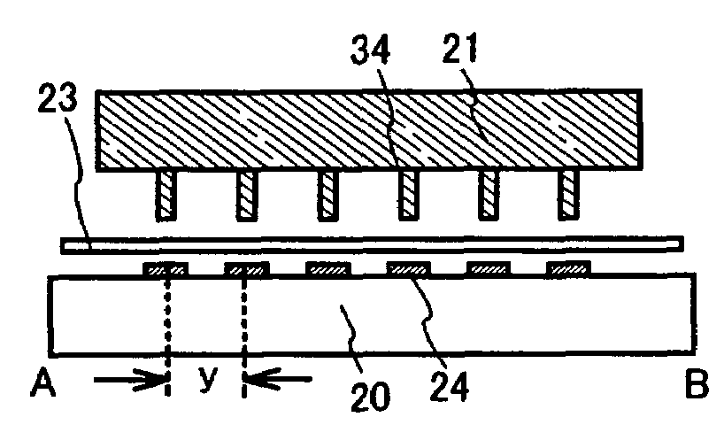
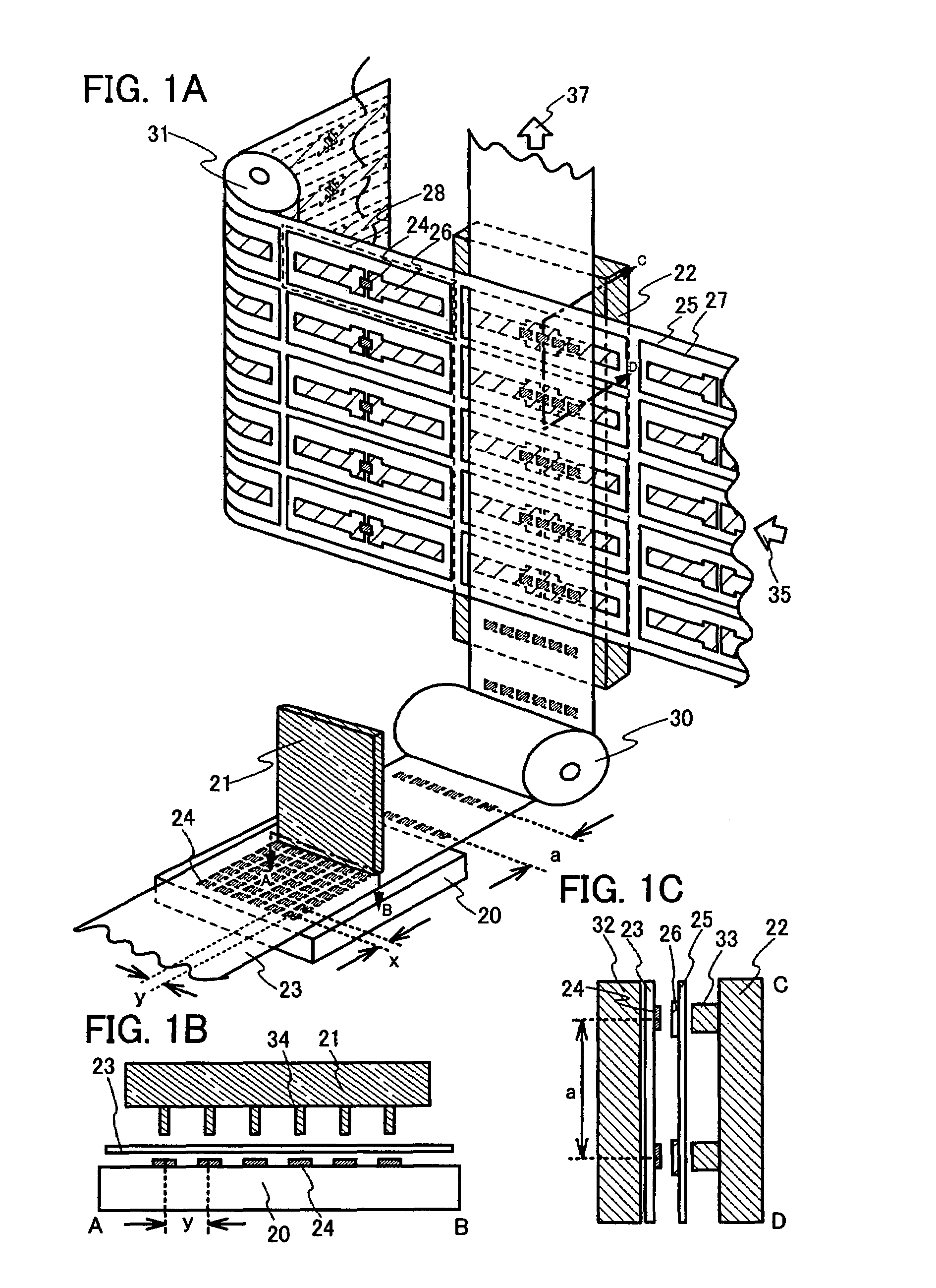
[0063]FIGS. 1A to 1C show modes of an attachment apparatus and a manufacturing apparatus of a semiconductor device of the present invention. The attachment apparatus includes a support unit over which first components are arranged, a first flexible substrate for holding the first components, and a pickup unit for temporarily attaching the first components arranged over the support unit to the first flexible substrate. In addition, the attachment apparatus includes a second flexible substrate over which second components are arranged, and a bonding unit for connecting the first components to the second components. Further, the attachment apparatus includes a first substrate transport unit having a first supply portion for supplying (feeding) the first flexible substrate and a first recovery portion for recovering (taking up) the first...
embodiment mode 2
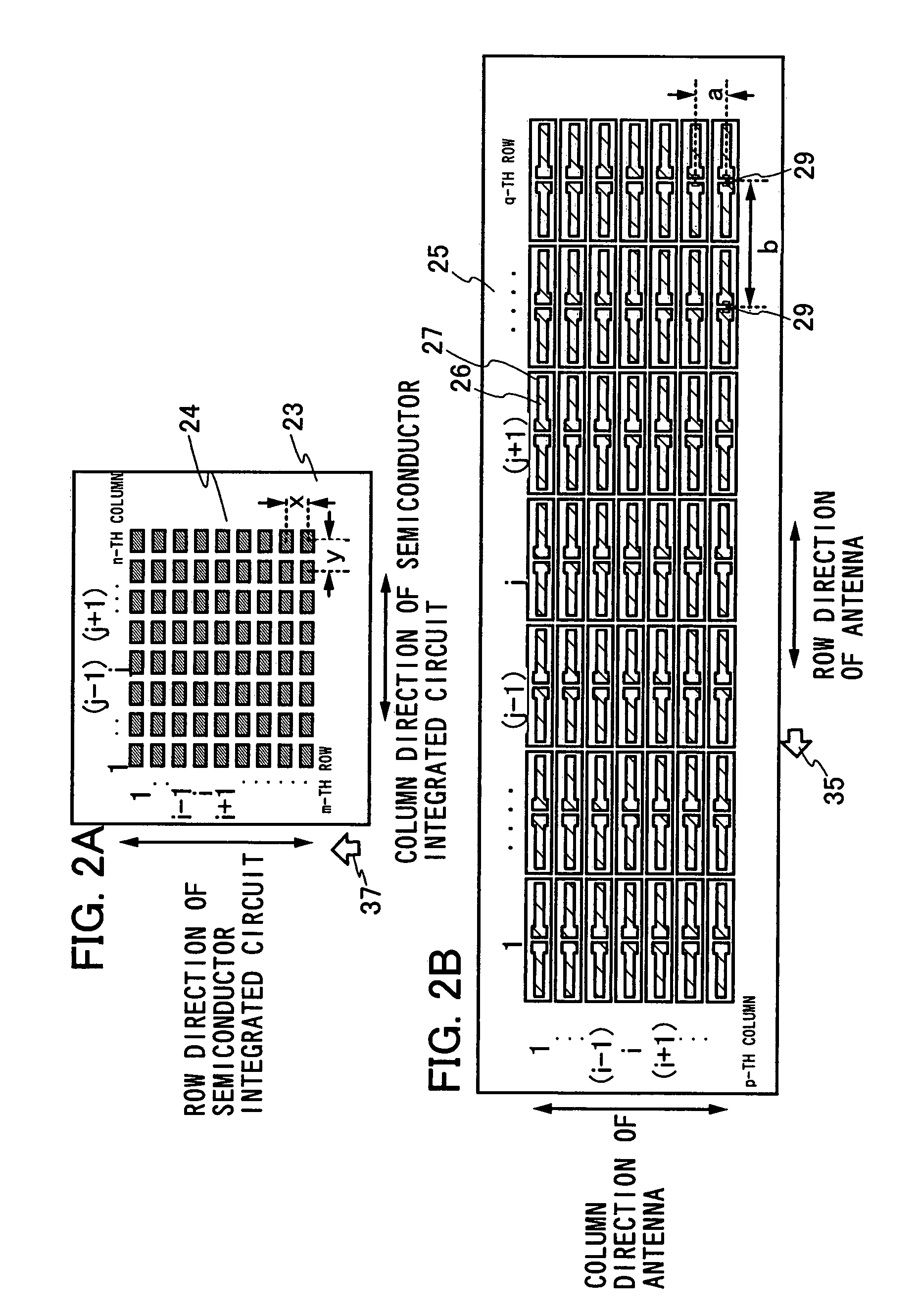
[0130]This embodiment mode describes a mode in which rows and columns of each of first components and second components are arranged to intersect with each other at a certain angle θ.
[0131]In an attachment apparatus to be described in this embodiment mode, surfaces of a first substrate and a second substrate face each other, and longer sides thereof, that is, the directions of movement thereof intersect with each other at 90° as shown in FIGS. 1A to 1C. As for first components arranged in a matrix with m rows and n columns, the rows and the columns intersect with each other at arc tan(y / x). In addition, as for second components arranged in a matrix with q rows and p columns, the rows and the columns intersect with each other at arc tan(y / a). Note that without limitation to the above structure, the rows and the columns of the first components arranged in the matrix with m rows and n columns may intersect with each other at 90°; the rows and the columns of the second components arrang...
embodiment 1
[0155]This embodiment describes a manufacturing process of a semiconductor device capable of contactless data transmission with reference to FIGS. 15A to 17B.
[0156]As shown in FIG. 15A, a peeling layer 1202 is formed over a substrate 1201; an insulating layer 1203 is formed over the peeling layer 1202; a thin film transistor 1204 and an interlayer insulating layer 1205 for insulating a conductive layer of the thin film transistor are formed over the insulating layer 1203; and source and drain electrodes 1206 connected to a semiconductor layer of the thin film transistor are formed. Next, an insulating layer 1207 which covers the thin film transistor 1204, the interlayer insulating layer 1205, and the source and drain electrodes 1206 is formed, and a conductive layer 1208 connected to the source or drain electrode 1206 with the insulating layer 1207 interposed therebetween is formed.
[0157]As the substrate 1201, a glass substrate, a quartz substrate, a metal substrate or a stainless-s...
PUM
 Abstract
Description
Claims
Application Information
 - R&D
- Intellectual Property
- Life Sciences
- Materials
- Tech Scout
- Unparalleled Data Quality
- Higher Quality Content
- 60% Fewer Hallucinations
Browse by: Latest US Patents, China's latest patents, Technical Efficacy Thesaurus, Application Domain, Technology Topic, Popular Technical Reports.
© 2025 PatSnap. All rights reserved.Legal|Privacy policy|Modern Slavery Act Transparency Statement|Sitemap|About US| Contact US: help@patsnap.com