
Structures and methods for measuring beam angle in an ion implanter

a technology of beam angle and ion implanter, which is applied in the field of ion implantation, can solve the problems of difficult control of commercial ion implanters, various accuracy limitations, and difficult measurement of ion beam angle at low energies, so as to facilitate semiconductor apparatus fabrication, improve angular uniformity, and improve the effect of beam angl

Active Publication Date: 2010-06-01
AXCELIS TECHNOLOGIES
View PDF2 Cites 0 Cited by
  • Summary
  • Abstract
  • Description
  • Claims
  • Application Information

AI Technical Summary

Benefits of technology

The present invention is about a method and apparatus for measuring the angle of ion beams during semiconductor device fabrication. This is achieved by using composite pillars or slots on an insulating layer, which allow ion beams to penetrate and measure the resistivity of the layer before and after implantation. This information is used to adjust the ion beam angle and improve the uniformity of the beam angle during implantation. The invention can provide better control over the ion beam angle and help achieve better process results.

Problems solved by technology

Ion beam angle at low energies is difficult to measure using conventional metrology.
However, these techniques have various limitations in terms of accuracy.
However, there is an interest in measuring ion angles for ion beams having energies below 5 keV because it is of practical importance in building advanced semiconductor apparatus and it is the energy range that is typically the most difficult for a commercial ion implanter to control in terms of ion beam angle, for example.
If the ion channeling techniques do not work because of the energy levels involved, manufacturers are forced to build some type of structure that is no longer a bare wafer.

Method used


Image

  • Structures and methods for measuring beam angle in an ion implanter
  • Structures and methods for measuring beam angle in an ion implanter
  • Structures and methods for measuring beam angle in an ion implanter

Examples


Embodiment Construction

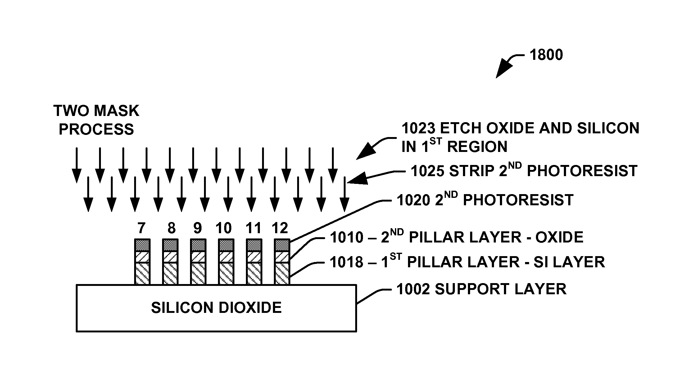
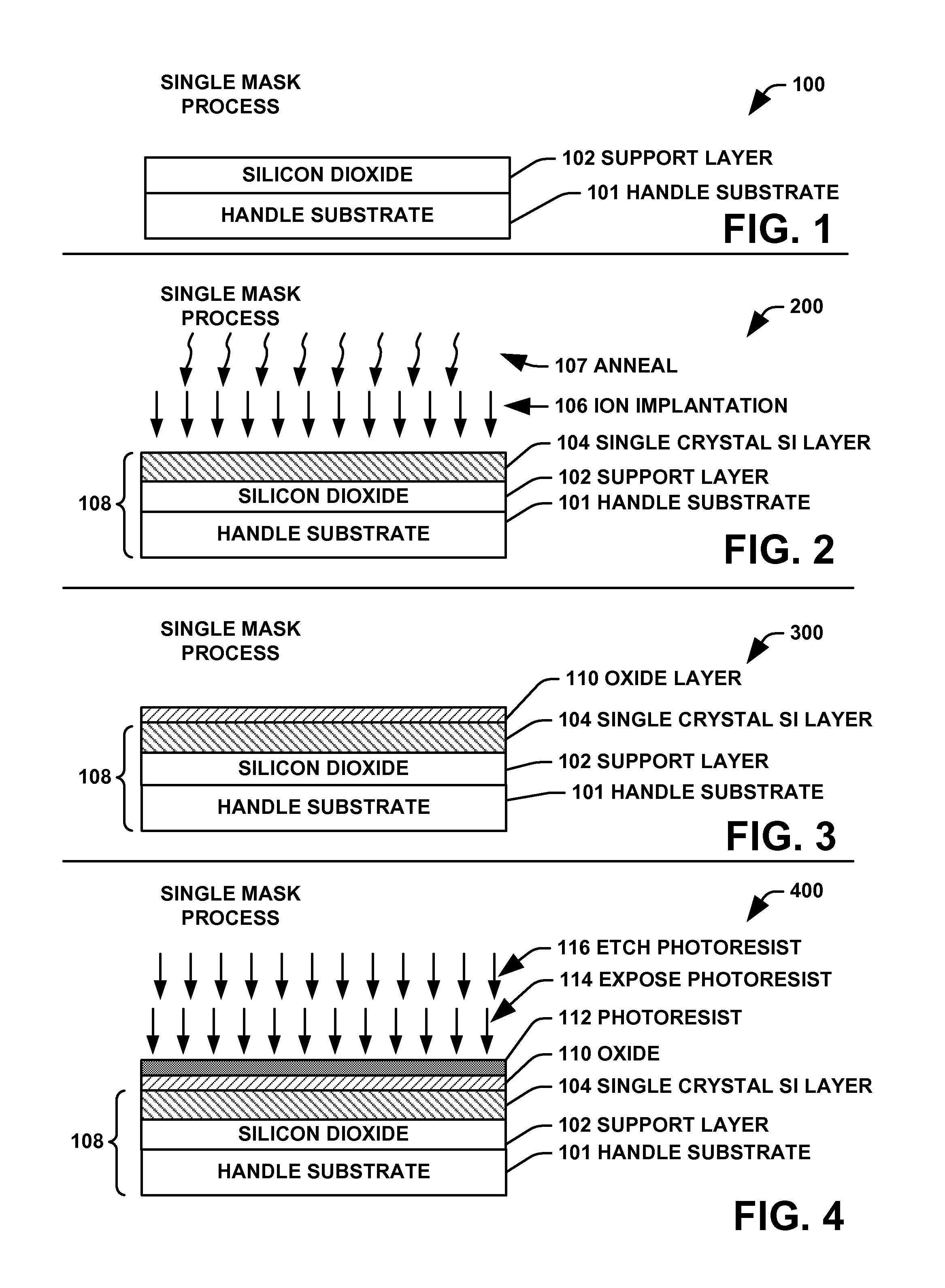
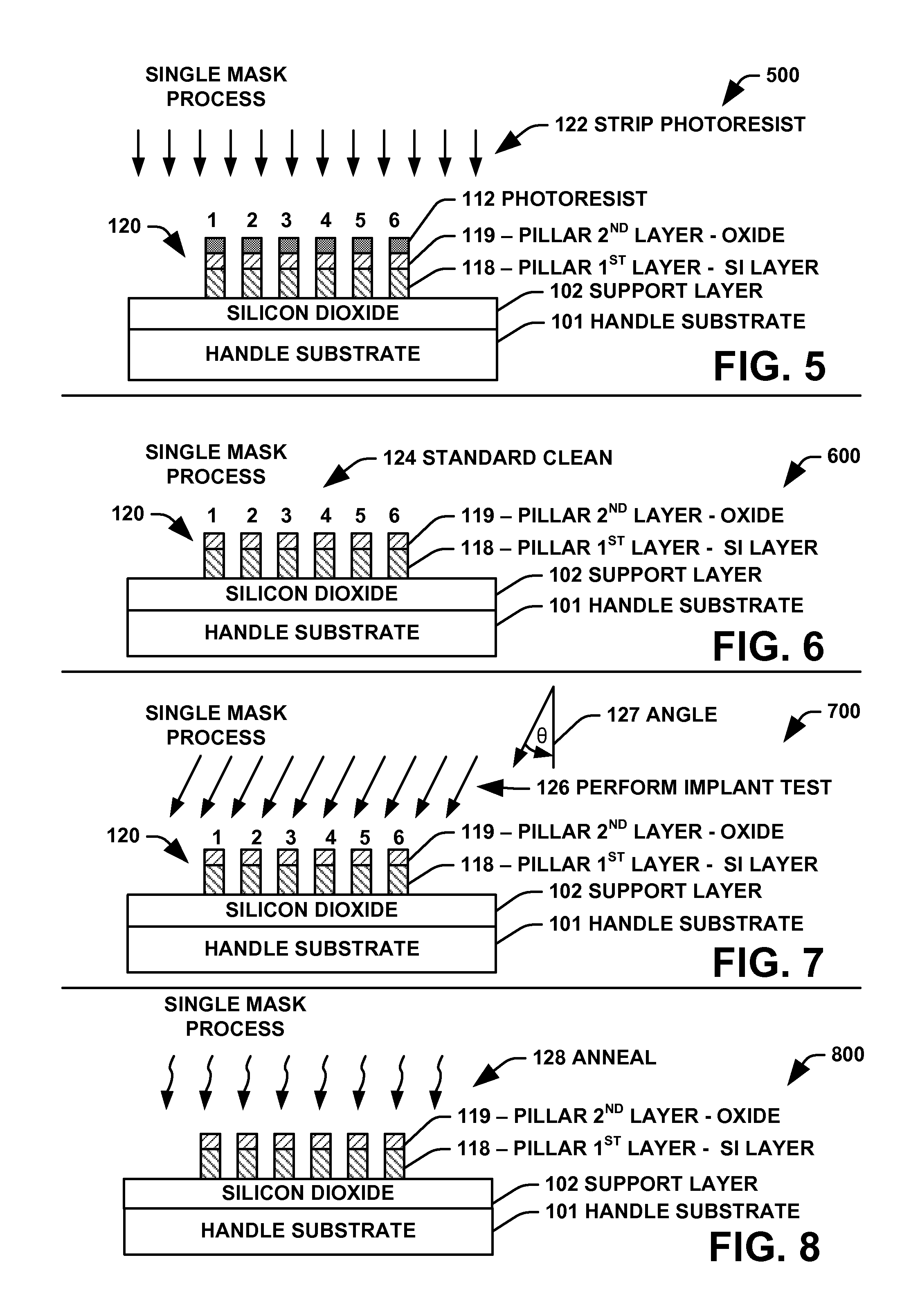
[0032]The present invention will now be described with reference to the attached drawings, wherein like reference numerals are used to refer to like elements throughout. It will be appreciated by those skilled in the art that the invention is not limited to the exemplary implementations and aspects illustrated and described hereinafter. For the sake of providing a clear description of the invention, the structures and the methods will be described in connection with periodic pillar structures. However, it is to be expressly understood that this description is not intended to be self-limiting in any manner. It is contemplated that the concepts of the present invention may be utilized with other types and configurations of periodic structures (e.g., trenches and the like) without departing from the spirit and the scope of the invention

[0033]The present invention facilitates semiconductor apparatus fabrication by measuring ion beam angles utilizing high aspect ratio pillars of silicon ...


PUM

PropertyMeasurementUnit
energyaaaaaaaaaa
thickaaaaaaaaaa
lengthaaaaaaaaaa

Abstract

The present invention involves an ion beam angular measurement apparatus for providing feedback for a predetermined set ion beam angle comprising an arrangement of composite pillars formed on an insulating material and wherein the composite pillars selectively allow ion beams to penetrate a first layer of a pillar, wherein resistivity measurements are taken for each of the composite pillars before and after test ion beam implantation and wherein the resistivity measurements yield information relating to an angle of the ion beam during test.

Description

FIELD OF INVENTION[0001]The present invention relates generally to ion implantation, and, more particularly, to a systems and methods for measuring beam angle in an ion implanter.BACKGROUND OF THE INVENTION[0002]Ion implantation is a physical process, as opposed to diffusion, which is a chemical process that is employed in semiconductor apparatus fabrication to selectively implant dopant into semiconductor workpieces and / or wafer material. Thus, the act of implanting does not rely on a chemical interaction between a dopant and the semiconductor material. For ion implantation, dopant atoms / molecules are ionized and isolated, sometimes accelerated or decelerated, formed into a beam, and swept across a workpiece or wafer. The dopant ions physically bombard the workpiece, enter the surface and come to rest below the surface and typically come to rest below the workpiece surface in the crystalline lattice structure thereof.[0003]An ion implantation system is a collection of sophisticated...

Claims


Application Information

Patent Timeline
Patent Type & Authority Patents(United States)
IPC IPC(8): G01N21/00
CPCH01J37/244H01J37/3171H01L22/34H01L21/26586H01L22/14H01J2237/24507H01J2237/24528
Inventor RUBIN, LEONARD M.BERRY, IVANCLASS, WALTER
Owner AXCELIS TECHNOLOGIES
Learn More