Resistance change memory device

a memory device and resistance change technology, applied in the field of resistance change memory devices, can solve the problems of not easy to further carry forward the miniaturization, not easy to access the plural cell array at a time, and difficult to read/write circuits

Inactive Publication Date: 2010-06-01
TOSHIBA MEMORY CORP
View PDF12 Cites 96 Cited by
  • Summary
  • Abstract
  • Description
  • Claims
  • Application Information

AI Technical Summary

Problems solved by technology

However, it is not easy to further carry forward the miniaturization.
However, conventionally proposed cell array stacking methods are such that planar cell arrays are simply stacked.
Therefore, it is not easy to access to plural cell arrays at a time.
In order to increase the capacity of such the phase change memory, how to integrally form a cell array and a read / write circuit thereof becomes an important technical issue.
Additionally, how to design the read / write circuit capable to perform high-speed data input / output is also becomes an important technical issue.

Method used


Image

  • Resistance change memory device
  • Resistance change memory device
  • Resistance change memory device

Examples


Embodiment Construction

[0045]Referring to the drawings, embodiments of this invention will be described bellow.

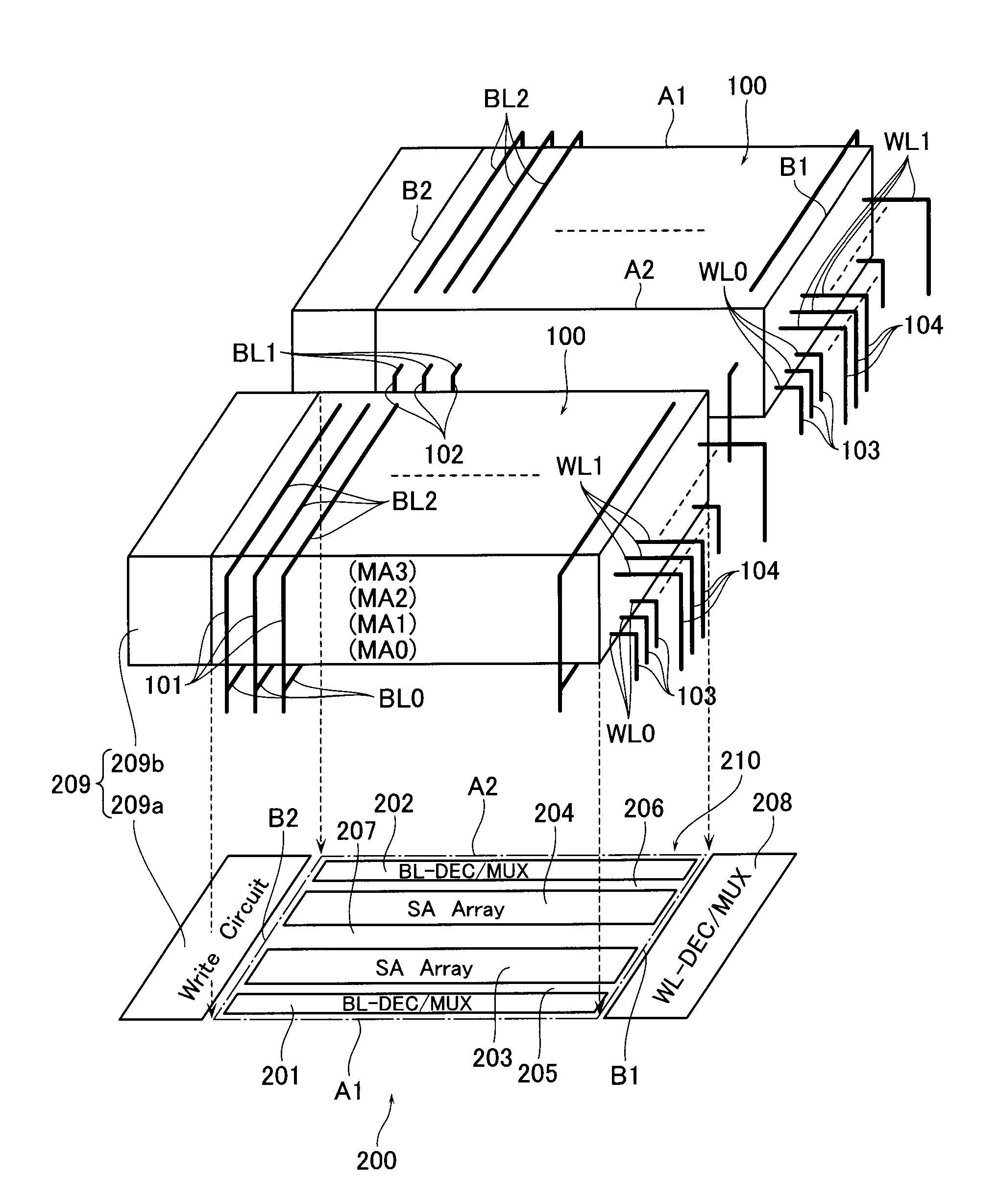
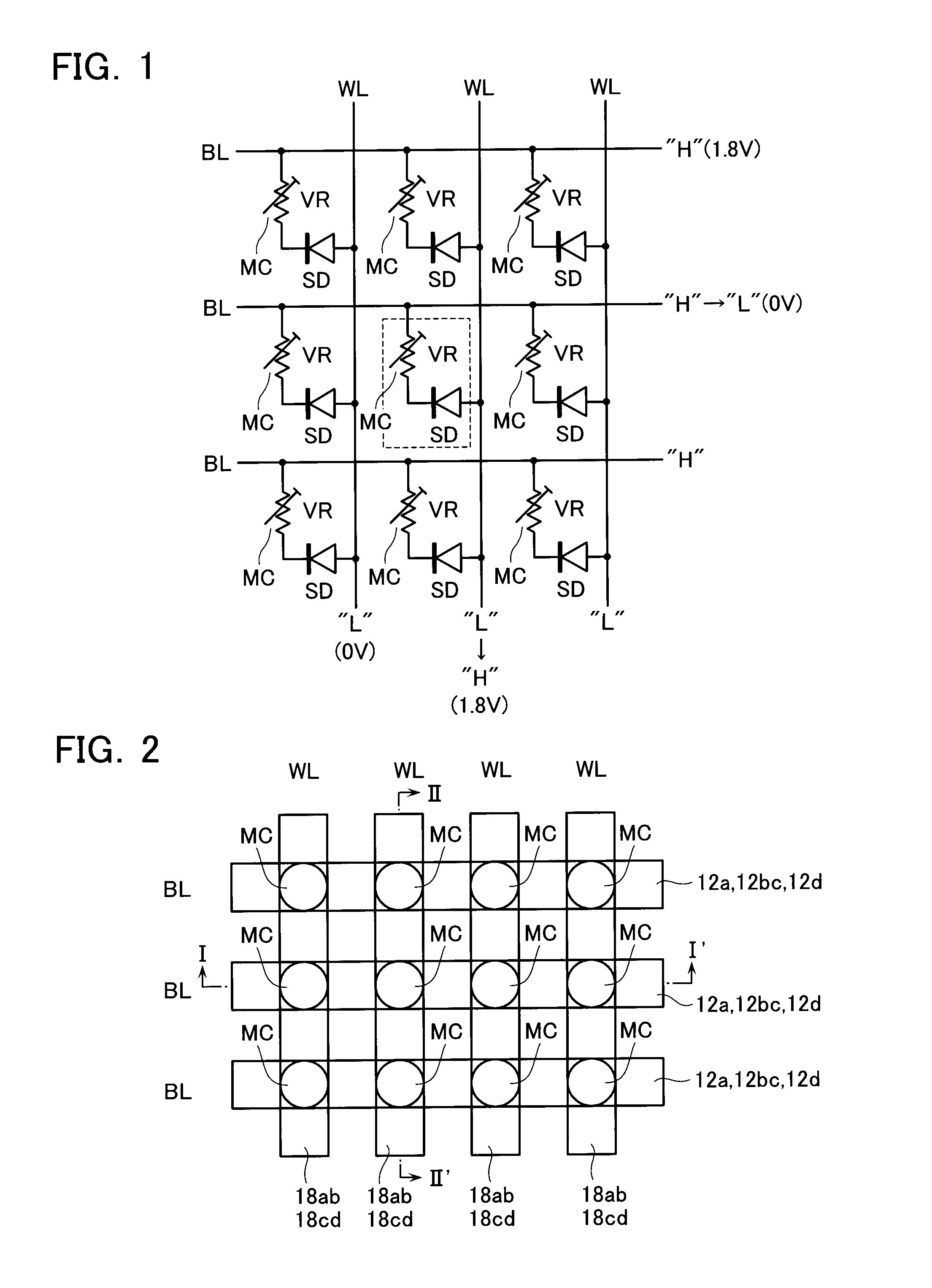
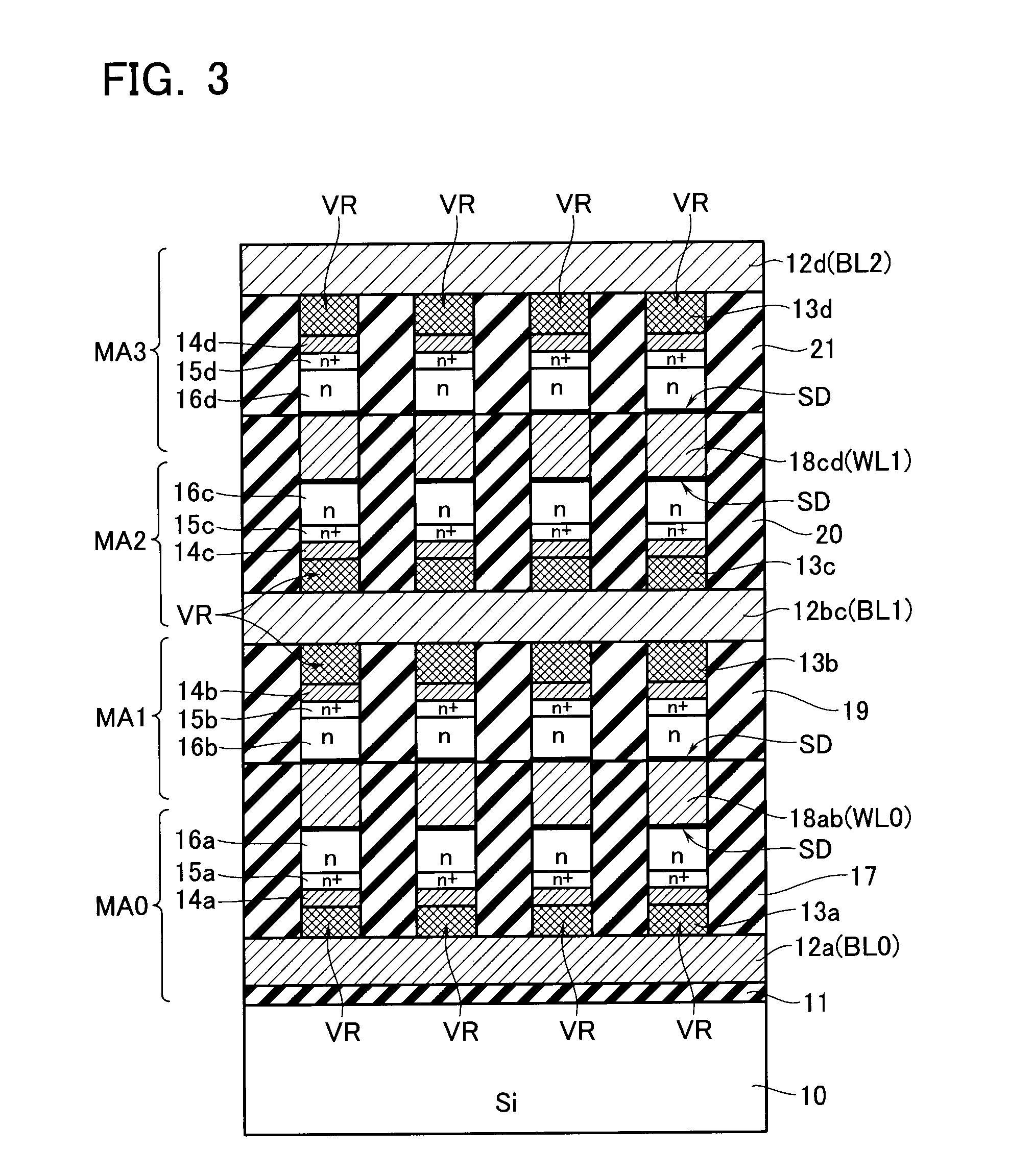
[0046]FIG. 1 shows a cell array of a phase change memory in accordance with an embodiment, with respect to a 3×3 cell matrix. A plurality of word lines WL are provided in parallel, and a plurality of bit lines BL are provided to cross the word lines WL.

[0047]Memory cells MC are laid out at the respective crossing points of these lines. The memory cell MC is a series-connection circuit of a variable resistive element VR and a diode SD. The variable resistive element VR is formed of chalcogenide and is operable to store therein a resistance value determined due to a phase transition between its crystalline and amorphous states as a binary data in a nonvolatile manner.

[0048]Although the diode SD is a Schottky diode in a preferable case of this embodiment, a PN-junction diode is alternatively usable. One end of the memory cell MC is connected to a bit line BL, and the other end is connected to a word...


PUM


Abstract

A resistance change memory device including: a semiconductor substrate; cell arrays stacked above the substrate, each having memory cells, bit lines and word lines; a read / write circuit formed on the semiconductor substrate; first and second vertical wirings disposed to connect the bit lines to the read / write circuit; and third vertical wirings disposed the word lines to the read / write circuit. The memory cell includes a variable resistance element for storing as information a resistance value, which has a recording layer composed of a composite compound containing at least two types of cation elements, at least one type of the cation element being a transition element having “d” orbit, in which electrons are incompletely filled, the shortest distance between adjacent cation elements being 0.32 nm or less.

Description

BACKGROUND OF THE INVENTION[0001]1. Field of the Invention[0002]This invention relates to a resistance change memory device, which stores a resistance value determinable by a resistance change of memory material in a non-volatile manner.[0003]2. Description of the Related Art[0004]EEPROM flash memories are known in the prior art as large capacitive and multi-functional non-volatile semiconductor memories. In this kind of semiconductor memories, miniaturized circuits with a minimal size of 100 nm or less has been achieved in the memory plane.[0005]In order to further increase the memory capacity, it is required to further the miniaturization for increasing a cell number in a unit area. However, it is not easy to further carry forward the miniaturization.[0006]Some approaches have been examined to increase the memory capacity without carrying forward the miniaturization such as, for example, to package plural memory chips as being stacked, or form a three-dimensional memory chip with ...

Claims


Application Information

Patent Timeline
Patent Type & Authority Patents(United States)
IPC IPC(8): G11C11/00
CPCG11C5/02H01L27/2481G11C13/0004G11C13/0007H01L27/2409G11C7/18G11C2213/31G11C2213/71G11C2213/72H01L45/06H01L45/085H01L45/1233H01L45/1253H01L45/126H01L45/147H10B63/84H10B63/20H10N70/245H10N70/841H10N70/8413H10N70/8836H10N70/231H10N70/826
Inventor TODA, HARUKIKUBO, KOICHI
Owner TOSHIBA MEMORY CORP
Why Eureka
Try Eureka