Stack package and semiconductor module implementing the same

a technology of semiconductor modules and stack packages, applied in the direction of switchgear arrangements, electrical apparatus contruction details, printed circuit non-printed electric components association, etc., can solve the problems of affecting the efficiency of chip stacking, and affecting the yield of chip stacking techniques

Inactive Publication Date: 2010-06-08
SAMSUNG ELECTRONICS CO LTD
View PDF12 Cites 2 Cited by
  • Summary
  • Abstract
  • Description
  • Claims
  • Application Information

AI Technical Summary

Problems solved by technology

For example, such technologies may involve fine line-widths and / or a substantial development time.
However, the chip stacking techniques may suffer from a decreased yield.
Here, repair work may not be possible.
On the one hand, the unit package stacking technique may result in a stack package that is thicker than one manufactured by stacking chips.
The application of heat may cause thermal stresses in the components of the stack package 10.
Such thermal stresses may damage the components.
For example, thermal stresses may cause defects, such as splitting of conductive bumps and / or short circuits between adjacent conductive bumps.
Package defects may occur more frequently as the number of unit packages in the stack increases.
Thus, during processes that may involve the application of heat (e.g., the stacking of unit packages), substrate warpage may occur.
Substrate warpage may cause defects.
Accordingly, the repair process may cause the aforementioned defects.
Thus, the semiconductor chip may be susceptible to damage from external forces.

Method used


Image

  • Stack package and semiconductor module implementing the same
  • Stack package and semiconductor module implementing the same
  • Stack package and semiconductor module implementing the same

Examples


Embodiment Construction

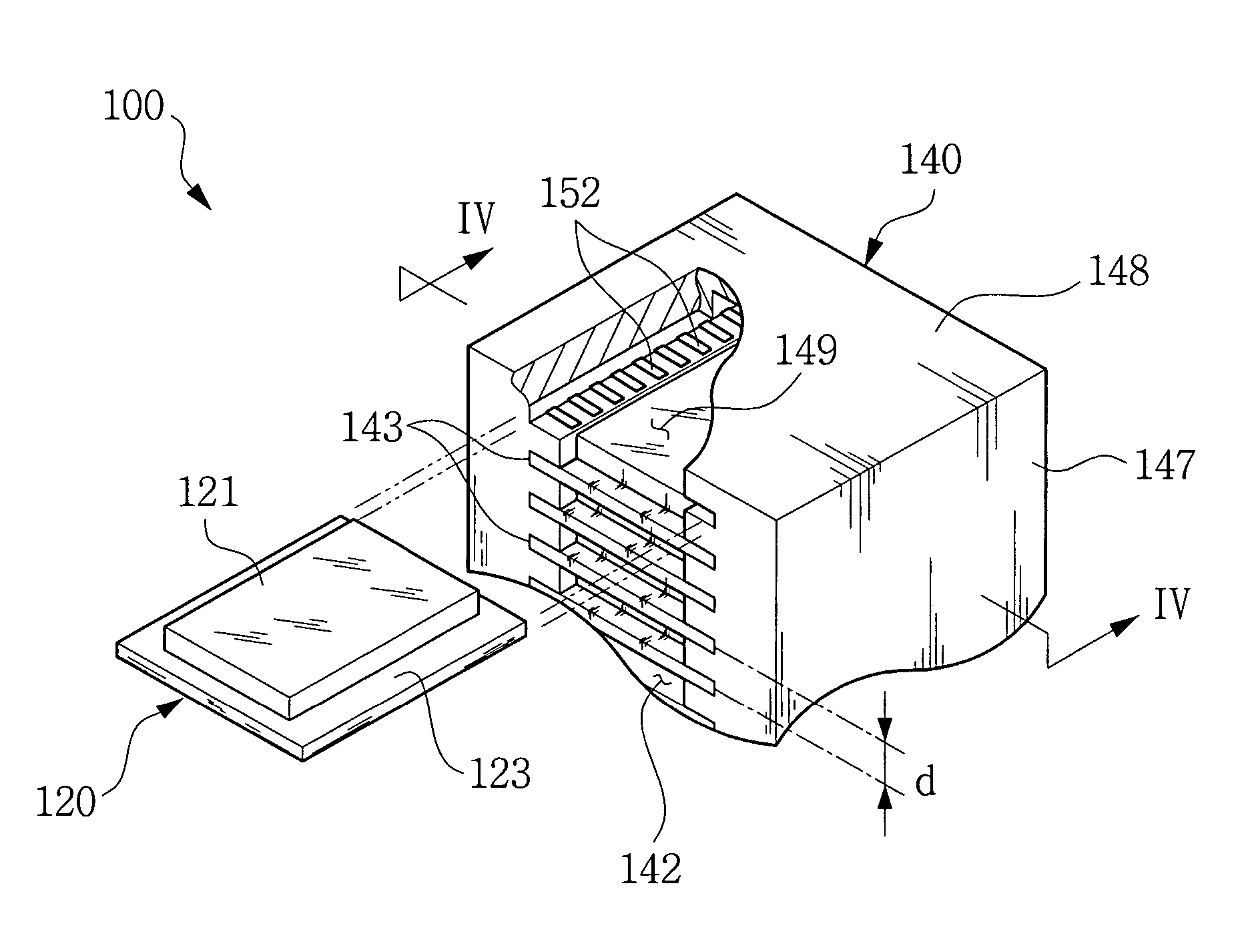
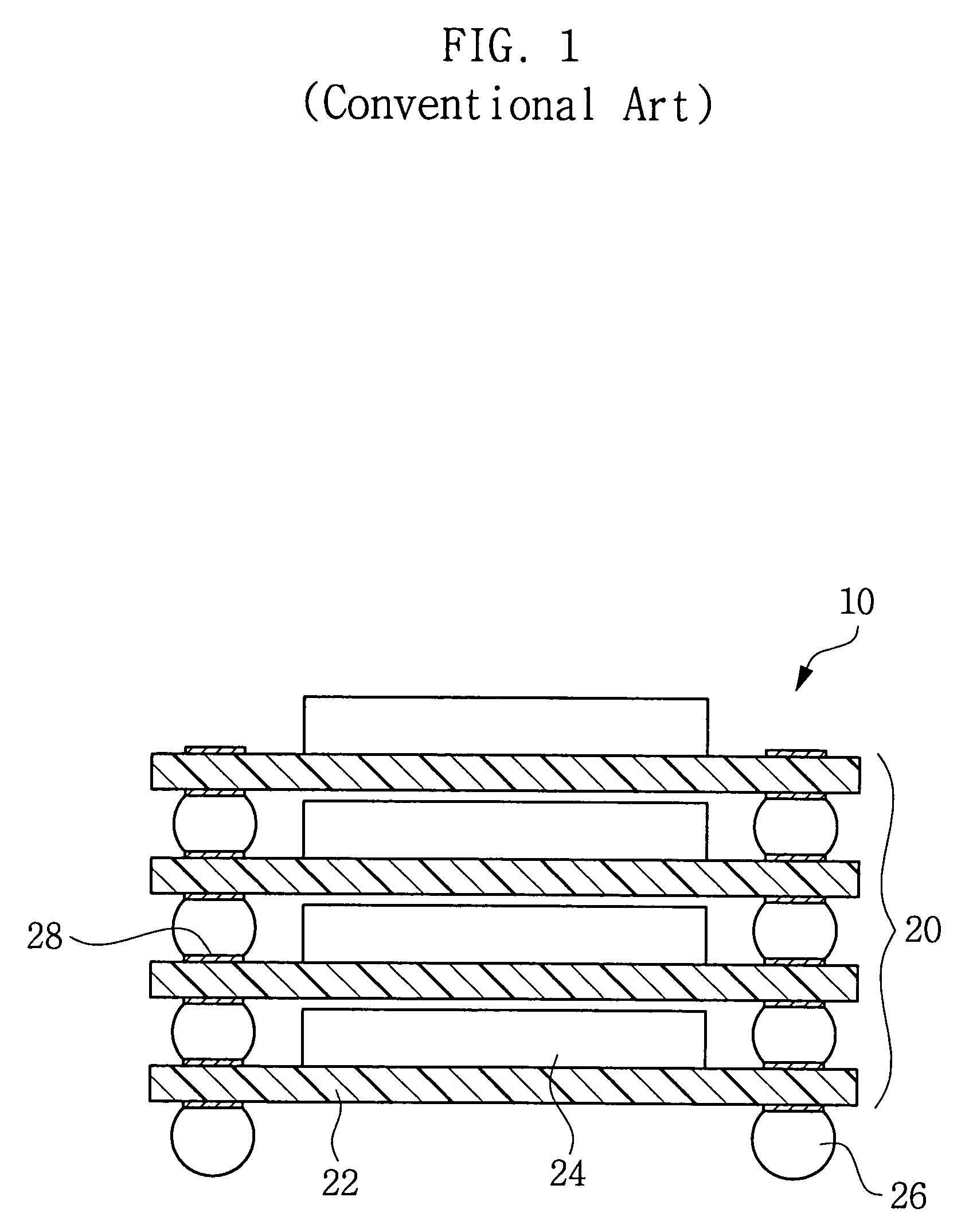
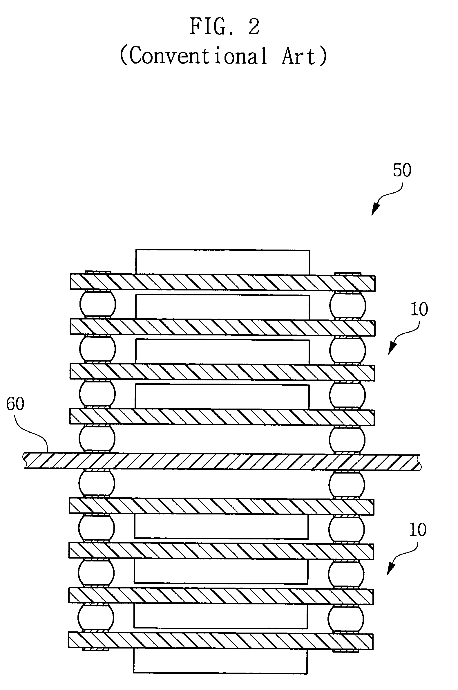
[0036]Example, non-limiting embodiments of the present invention will be described in detail with reference to the accompanying drawings. This invention may, however, be embodied in many different forms and should not be construed as limited to the example embodiments set forth herein. Rather, the disclosed embodiments are provided so that this disclosure will be thorough and complete, and will fully convey the scope of the invention to those skilled in the art. The principles and features of this invention may be employed in varied and numerous embodiments without departing from the scope of the invention.

[0037]An element is considered as being mounted (or provided) “on” another element when mounted or provided) either directly on the referenced element or mounted (or provided) on other elements overlaying the referenced element. Throughout this disclosure, spatial terms such as “upper,”“lower,”“above” and “below” (for example) are used for convenience in describing various element...


PUM


Abstract

The stack package may have a structure in which unit packages may be inserted into slots of a receiving substrate. The unit package may have a plurality of connecting pads. The receiving substrate may have substrate pads, which may be electrically connected to the connecting pads of the unit packages inserted in the slots by mechanical contact. The slots may be provided at regular vertical intervals so that the unit packages may be stacked in the vertical direction. A semiconductor module may include stack packages installed on at least one surface of a module substrate.

Description

PRIORITY STATEMENT[0001]This U.S. non-provisional application claims benefit of priority under 35 U.S.C.§119 from Korean Patent Application No. 2005-60730, filed on Jul. 6, 2005, the entire contents of which are incorporated herein by reference.BACKGROUND[0002]1. Field of the Invention[0003]Example embodiments of the present invention relate to a semiconductor device and, more particularly, to a stack package having a plurality of unit packages that may be inserted into a receiving substrate to be stacked and electrically connected to each other, and a semiconductor module that may implement the same.[0004]2. Description of the Related Art[0005]The electronic industry may seek to provide products having (for example) characteristics of light-weight, miniaturization, high speed, multifunction, high performance, high reliability and low production cost. Packaging may be one technology area that may enable design of such a product. One packaging technique may provide a chip scale packa...

Claims


Application Information

Patent Timeline
Patent Type & Authority Patents(United States)
IPC IPC(8): H01L23/02H01L23/34
CPCH01L25/105H01L25/0657H01L2224/06136H01L2224/32145H01L2224/4824H01L2224/49109H01L2924/01079H01L2924/15311H01L2224/06135H01L2224/0401H01L2225/1005H01L2224/73215H01L2224/73204H01L2224/32225H01L2225/107H01L2225/1023H01L2924/3511H01L2224/73265H01L2224/16225H01L2924/00012H01L2224/48227H01L2924/00H01L24/73H01L23/12
Inventor YOON, TAE-SUNG
Owner SAMSUNG ELECTRONICS CO LTD
Why Eureka
Try Eureka