Wafer process flow for a high performance MEMS accelerometer

a technology of accelerometer and process flow, which is applied in the direction of speed/acceleration/shock measurement, measurement devices, instruments, etc., can solve the problems of reducing sensitivity, reducing the total mass of the plate, and limited resolution of high-performance accelerometers

Inactive Publication Date: 2010-06-15
ROSEMOUNT AEROSPACE
View PDF36 Cites 61 Cited by
  • Summary
  • Abstract
  • Description
  • Claims
  • Application Information

AI Technical Summary

Problems solved by technology

The resolution of high-performance accelerometers has been limited by thermomechanical Brownian noise of the sensor, which is dictated by the damping coefficient and the mass of the structure, as well as by the readout electronics.
However, increasing the center mass offset by the asymmetric shaping methods mentioned above may result in an increase in total mass of the plate, which leads to reduced resonant frequency and decreased sensitivity.
Increasing the center mass offset by asymmetric shaping may also result in a sacrifice of some of the dynamic g-range, which is defined by the separation distance between a stationary sensing element and the pendulous acceleration sens...

Method used


Image

  • Wafer process flow for a high performance MEMS accelerometer
  • Wafer process flow for a high performance MEMS accelerometer
  • Wafer process flow for a high performance MEMS accelerometer

Examples


Embodiment Construction

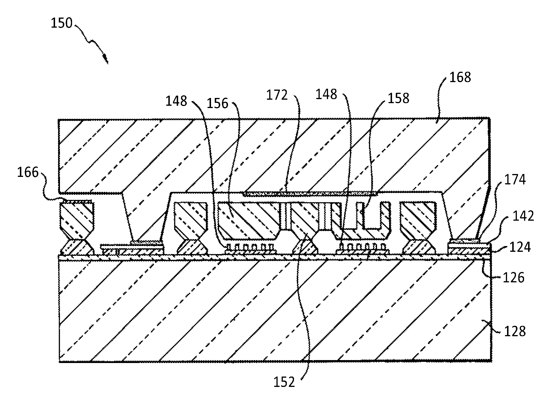
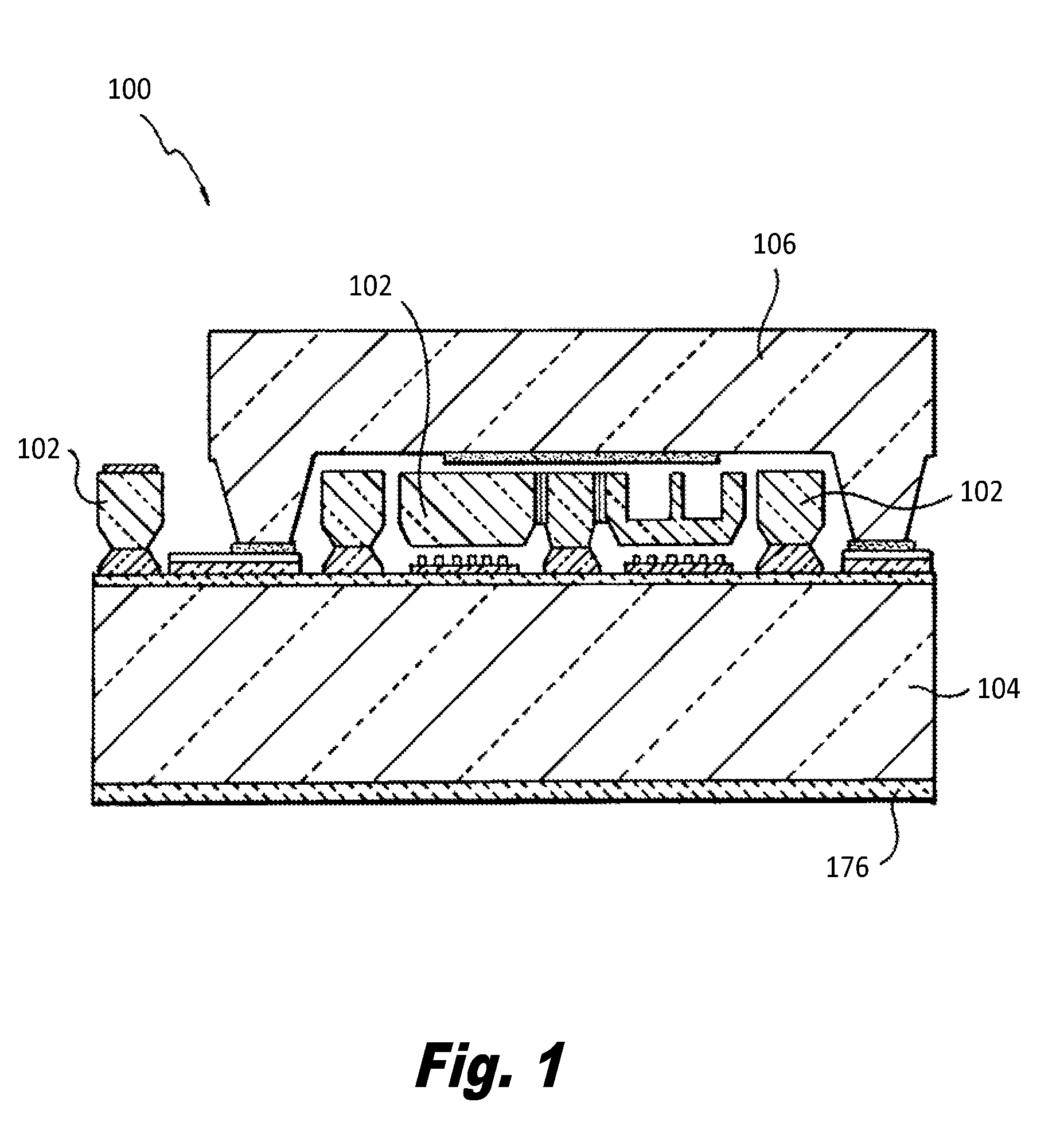
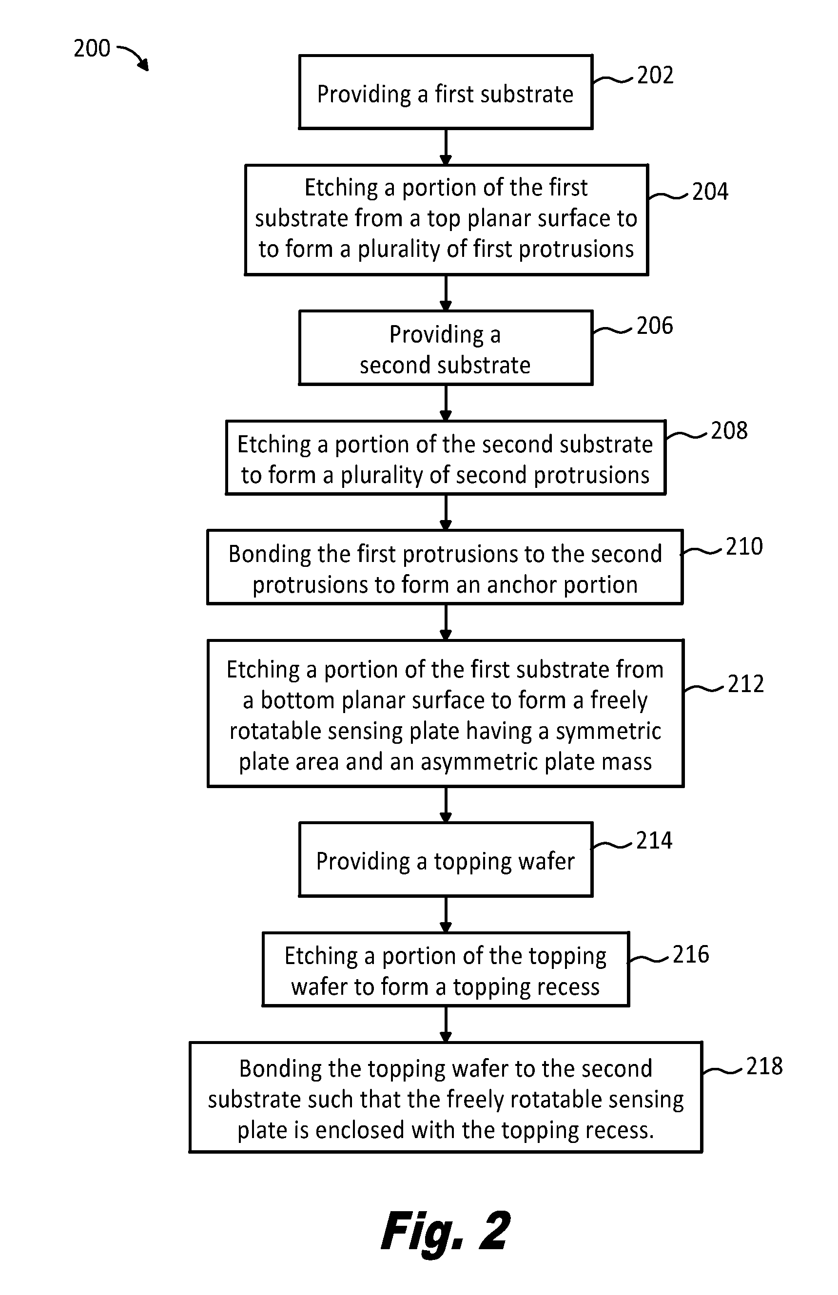
[0034]An exemplary fabrication process flow according to the present invention will now be described. A silicon on insulator (SOI) bottom electrode wafer with a thickness of about 5 μm is obtained. A shallow cavity is photo patterned and wet etched to a depth of 1.6 μm in the bottom electrode wafer, followed by a deep reactive ion etch (DRIE) to form bottom electrodes. A top electrode SOI wafer with a thickness of about 75 μm is etched by potassium hydroxide (KOH) to form a proof cavity with a channel depth of about 20 μm. The bottom electrode wafer and top electrode wafer are then fusion bonded to one another. A handle wafer of the top electrode wafer is then removed, leaving a 75 μm active layer. Finally, the active layer of the top electrode wafer can be photo patterned and released by DRIE etch to release a rotatable sensing plate and to form a hollow proof mass on one side of the sensing plate. The hollow proof mass, having a cavity between 50 an 55 μm deep, will be formed duri...


PUM


Abstract

A process for fabricating a pendulous accelerometer, including the steps of: providing a first substrate having a top planar surface, etching a portion of the first substrate to a first predetermined depth from the top planar surface to form a plurality of first protrusions, providing a second substrate, etching a portion of the second substrate to a second predetermined depth to form a plurality of second protrusions, bonding planar surfaces of the first protrusions to planar surfaces of the second protrusions, and etching a portion of the first substrate from an opposite side of the first substrate to a third predetermined depth equal to or greater than the difference between the total thickness of the first substrate and the first predetermined depth to form a freely rotatable sensing plate that includes a substantially hollow proof mass.

Description

BACKGROUND OF THE INVENTION[0001]1. Field of the Invention[0002]The present invention relates to fabrication processes for accelerometers and other force sensing devices, and more particularly to a fabrication process for producing a capacitive pendulous MEMS accelerometer with a symmetric plate area having an asymmetric plate mass.[0003]2. Description of Related Art[0004]High performance accelerometers with near micro-gravity resolution, high sensitivity, high linearity, and low bias drift are needed for a wide variety of applications, especially aerospace applications such as inertial navigation systems, guidance systems, and air data measurement systems. The resolution of high-performance accelerometers has been limited by thermomechanical Brownian noise of the sensor, which is dictated by the damping coefficient and the mass of the structure, as well as by the readout electronics.[0005]Fabrication technology plays a critical role in ensuring that large mass, large capacitance, a...

Claims


Application Information

Patent Timeline
IPC IPC(8): H01L21/00
CPCG01P15/0802G01P15/02
Inventor GUO, SHUWEN
Owner ROSEMOUNT AEROSPACE
Why Eureka
Try Eureka