Semiconductor device comprising chip on chip structure

a technology of semiconductor devices and chips, applied in the direction of semiconductor/solid-state device testing/measurement, semiconductor/solid-state device details, instruments, etc., can solve the problems of not being able to test the small chip alone, not being able to direct connect the external terminals of the small chip to the external terminals of the semiconductor device, and complicated soc process, etc., to second chips, reduce the number of test patterns and the like, and improve the operation margin of the first chip second

Active Publication Date: 2010-06-22
SOCIONEXT INC
View PDF13 Cites 14 Cited by
  • Summary
  • Abstract
  • Description
  • Claims
  • Application Information

AI Technical Summary

Benefits of technology

[0008]It is an object of the present invention to make it possible to test semiconductor chips independently in a semiconductor device constituted of stacked semiconductor chips.
[0009]It is another object of the present invention to supply power to the semiconductor chips independently and improve an operation margin of each of the semiconductor chips in a semiconductor device constituted of stacked semiconductor chips.
[0010]According to one aspect of the present invention, a first chip has a first element formed area, a first interconnection terminal connected to a circuit formed in the first element formed area, and a first external terminal connecting the circuit formed in the first element formed area to an exterior of the semiconductor device. A second chip has a second element formed area, a second interconnection terminal connected to a circuit formed in the second element formed area, and a second external terminal connecting the circuit formed in the second element formed area to the exterior of the semiconductor device. The second chip is disposed to face the first chip via the second interconnection terminal connected to the first interconnection terminal. The first and second external terminals are formed on surfaces of the first and second chips. The surfaces are on a same side of the first and second chips. Therefore, even after the first chip and the second chips are pasted together, it is possible to operate the first chip and the second chip for testing independently. Further, since test probes or the like can be brought into contact with the external terminals of the first chip and the second chip from the same side, it is possible to simultaneously test the first chip and the second chip. Moreover, using the first and second external terminals makes it possible to supply independent power supplies to the first and second chips respectively. This can accordingly improve operation margins of the first and second chips.

Problems solved by technology

A semiconductor process of the SoC is complicated and also costs high.
This does not allow the direct connection of external terminals of the small chip to external terminals of a semiconductor device.
Therefore, it is not possible to test the small chip alone if not through the large chip.
Further, it is not possible to supply power to the small chip if not through the large chip.

Method used


Image

  • Semiconductor device comprising chip on chip structure
  • Semiconductor device comprising chip on chip structure
  • Semiconductor device comprising chip on chip structure

Examples


first embodiment

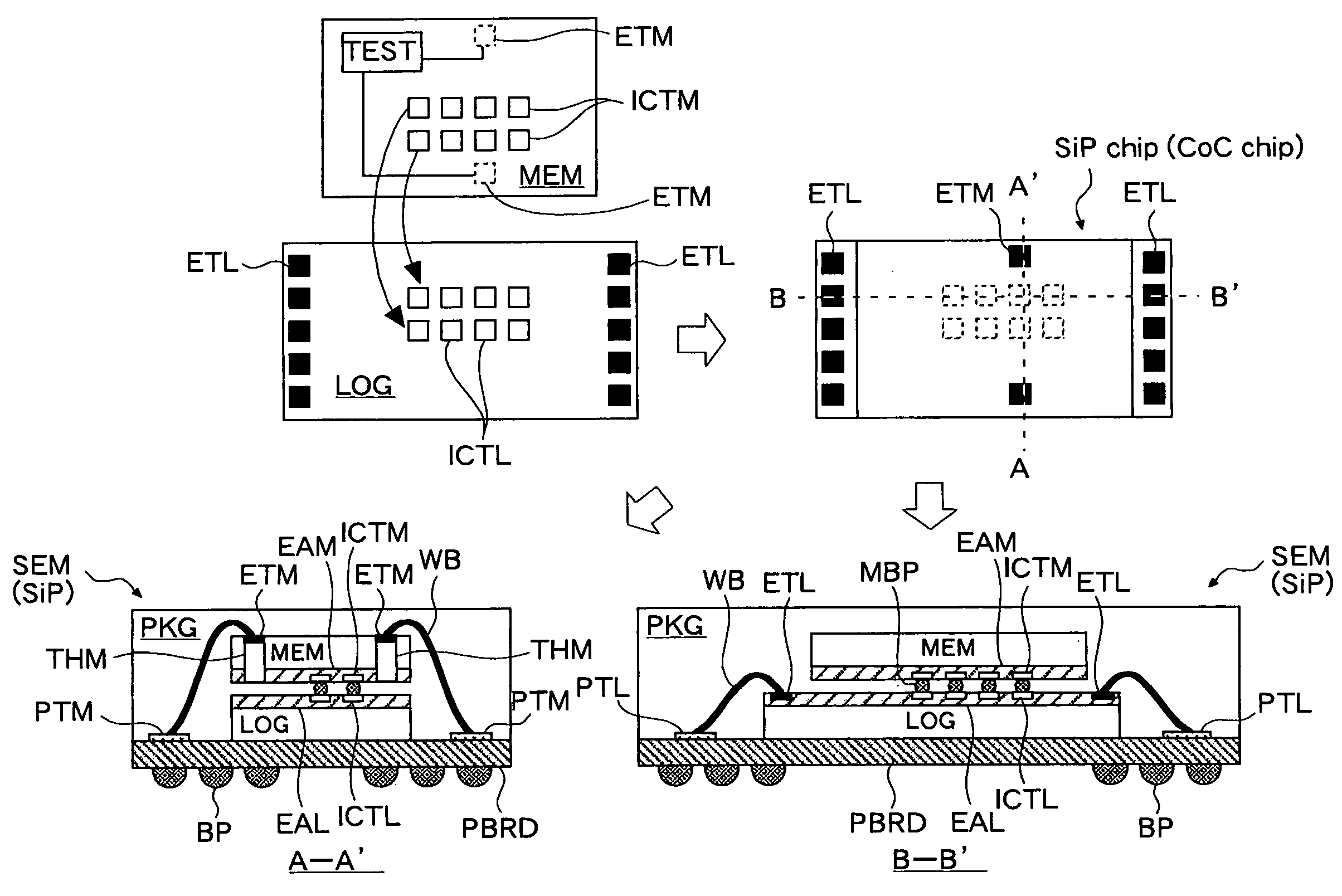
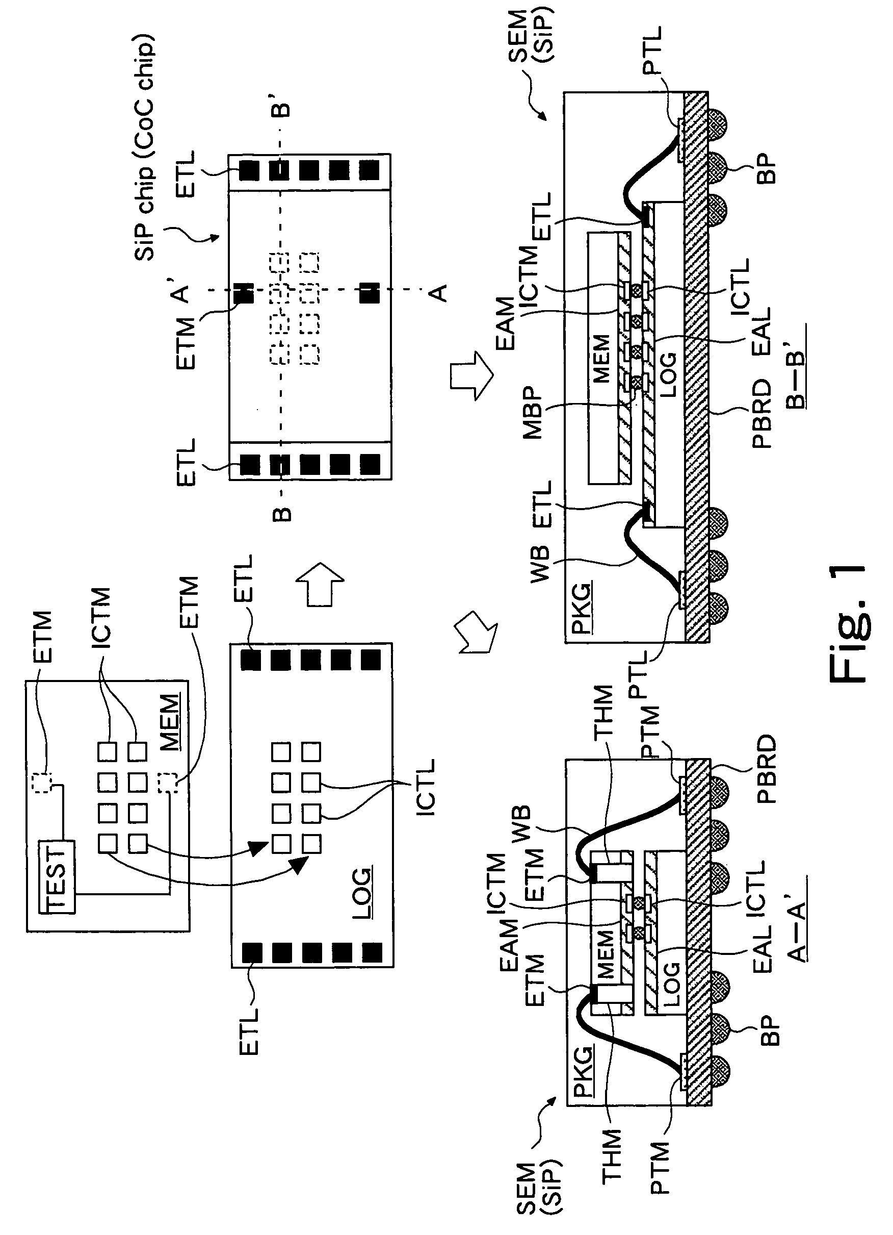
[0043]FIG. 1 shows a A semiconductor device SEM is formed by using a Chip on Chip (hereinafter, referred to as CoC) technology in such a manner that a memory chip MEM (second chip) is pasted on a logic chip LOG (first chip) to constitute a System in Package (hereinafter, also referred to as a SiP) and the SiP chip (CoC chip) is sealed in a package PKG.

[0044]A length in a lateral direction in FIG. 1 of the logic chip LOG is larger than that of the memory chip MEM, and the logic chip LOG has a plurality of external terminals ETL at positions (in the right and left directions in FIG. 1) not overlapping with the memory chip MEM. The memory chip MEM has two external terminals ETM at positions overlapping with the logic chip LOG. The logic chip LOG and the memory chip MEM have a plurality of interconnection terminals ICTL, ICTM, respectively, connected to each other.

[0045]The memory chip MEM has, for example, a test circuit TEST. The test circuit TEST is, for example, a BIST (Built-In Se...

ninth embodiment

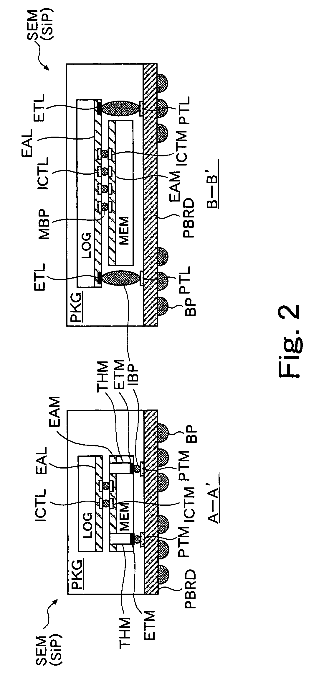
[0109]The ninth embodiment described above can also provide the same effects as those of the first, third, and sixteenth embodiments previously described. In addition, since no wiring layer WLYR is formed on the bad memory chips MEM, the time taken for the wiring process can be shortened and manufacturing cost of the semiconductor device SEM can be reduced.

[0110]The above first-sixth embodiments have described the examples where the test circuit TEST is formed on the memory chip MEM, and the external terminals ETM of the memory chip MEM are used as the test terminals. However, the present invention is not limited to such embodiments. The external terminals ETM are not limited to the test terminals but may be a power supply terminal and signal terminals. An example of another possible structure is to form a larger number of the external terminals ETM and use part of the external terminals ETM as the power supply terminal. In this case, by using the external terminals ETL, ETM, it is ...


PUM


Abstract

In a semiconductor device constituted of stacked semiconductor chips, in order to independently test each of the chips, a second chip is disposed to face a first chip, with a second interconnection terminal thereof connected to a first interconnection terminal of the first chip. First and second external terminals of the first and second chips are formed on surfaces of the first and second chips, the surface being on a same side of the first and second chips. Therefore, even after the first chip and the second chip are pasted together, it is possible to test the first chip and the second chip while operating them independently. Further, since test probes or the like can be brought into contact with the external terminals of the first chip and the second chip from the same side, it is possible to simultaneously test the first chip and the second chip.

Description

CROSS REFERENCE TO RELATED APPLICATION[0001]This application is based upon and claims the benefit of priority from Japanese Patent Application No. 2006-181978, filed on Jun. 30, 2006, the entire contents of which are incorporated herein by reference.BACKGROUND OF THE INVENTION[0002]1. Field of the Invention[0003]The present invention relates to a semiconductor device constituted of stacked semiconductor chips, adopting a Chip on Chip technology or the like.[0004]2. Description of the Related Art[0005]In recent years, a volume of data handled in system products such as mobile phones have dramatically increased. In accordance with this increase, capacities of semiconductor memories mounted in the system products have also increased and there has arisen a demand for semiconductor memories with a high data transfer rate. Generally, as a semiconductor device mounted in a system product of this type, there has been provided a System on Chip (SoC) in which a logic (controller) and memories...

Claims


Application Information

Patent Timeline
Patent Type & Authority Patents(United States)
IPC IPC(8): H01L29/40
CPCH01L25/0657H01L25/18H01L2924/1461H01L2224/16145H01L2224/48091H01L2224/48227H01L2224/73207H01L2224/73257H01L2225/0651H01L2225/06513H01L2225/06517H01L2225/06527H01L2225/06541H01L2225/06562H01L2225/06596H01L2924/01079H01L2924/15311H01L2924/3011H01L2224/1403H01L2224/14181H01L2924/00014H01L2225/06568H01L2225/06565H01L2924/1434H01L2224/45144H01L2224/32225H01L2224/73265H01L2924/0002G01R31/2884H01L22/32H01L25/0652H01L2224/0401H01L2224/04042H01L2224/0557H01L2224/16225H01L2224/1703H01L2924/1431H01L2924/00H01L2924/00012H01L2224/05552H01L24/73H01L2224/17181H01L2224/73253H01L2224/13025H01L2224/04073H01L23/12
Inventor UCHIDA, TOSHIYA
Owner SOCIONEXT INC
Why Eureka
Try Eureka