Semiconductor device

a technology of semiconductor devices and semiconductors, applied in semiconductor devices, semiconductor/solid-state device details, instruments, etc., to achieve the effect of facilitating equal wiring lengths, reducing the influence of crosstalk noise, and reducing capacitive coupling nois

Inactive Publication Date: 2010-07-06
RENESAS ELECTRONICS CORP
View PDF10 Cites 6 Cited by
  • Summary
  • Abstract
  • Description
  • Claims
  • Application Information

AI Technical Summary

Benefits of technology

[0009]In a semiconductor module on which a plurality of memory chips and data processor chips are mounted, equalization of wiring lengths between chips and reduction of noise in the wirings between the chips related to data and data strobe signals are further restricted by acceleration of the operating speed and lowering of the operating voltage. With respect to the above, the present inventors performed the following studies. In a structure where a plurality of wiring layers of the module board and a through hole for connecting the wiring layers are used in wiring chips, the through hole cannot be formed at any given position, which restricts the equalization of the wiring lengths between the chips. Further, when the acceleration proceeds, it is not desirable to exclude, as in Patent document 1, the address / command wiring from subjects of length equalization. Further, as described in Patent document 2, when connecting a bonding lead of a wiring pattern on the module board to a bonding pad of the chip with a wire, it is required to reduce the influence of crosstalk noise and capacitive coupling noise between wires. Particularly, when it is required to arrange a plurality of arrays of bonding leads with respect to the bonding pads arranged on one side of the chip, it is necessary to ease the influence of crosstalk and capacitive coupling not only between the right and left sides of the wires but also between upper and lower sides thereof.
[0010]It is therefore an object of the present invention is to provide a semiconductor device wherein it is easy to equalize wiring lengths between chips not only of the data system but also of the address system.
[0011]Another object of the present invention is to provide a semiconductor device wherein it is possible to ease the influence of crosstalk noise and capacitive coupling noise between the data system wirings of chips.

Problems solved by technology

Further, when the acceleration proceeds, it is not desirable to exclude, as in Patent document 1, the address / command wiring from subjects of length equalization.

Method used


Image

  • Semiconductor device
  • Semiconductor device
  • Semiconductor device

Examples


Embodiment Construction

1. Summary of Embodiments

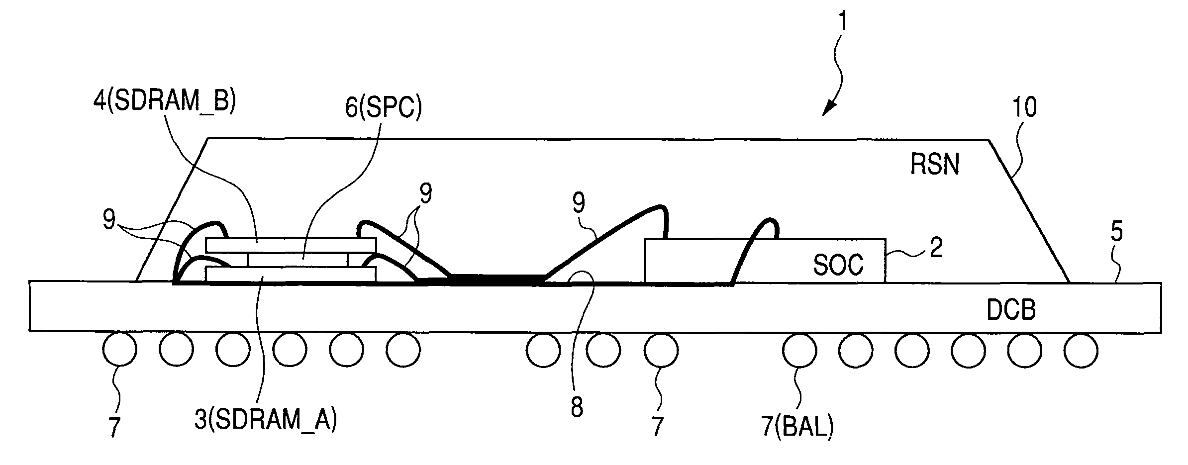
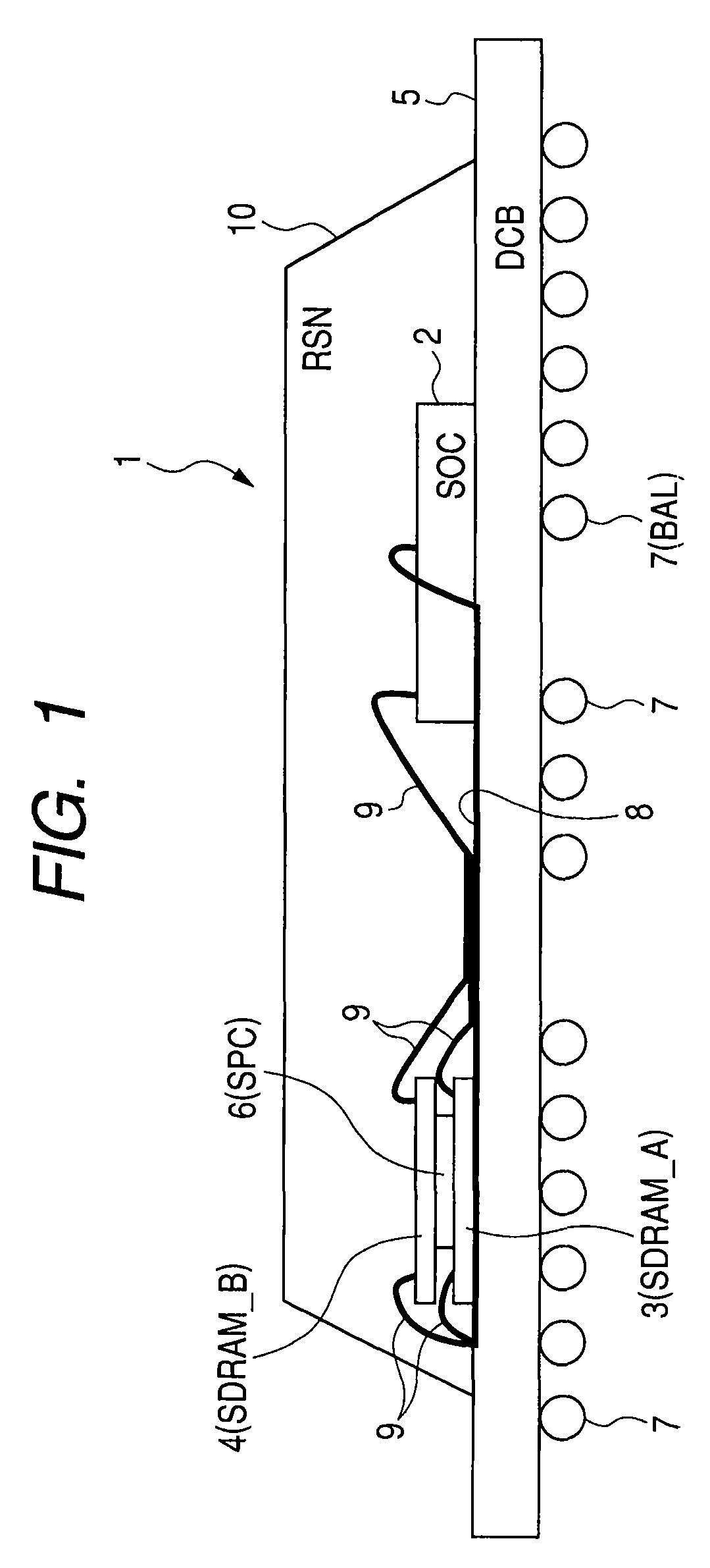
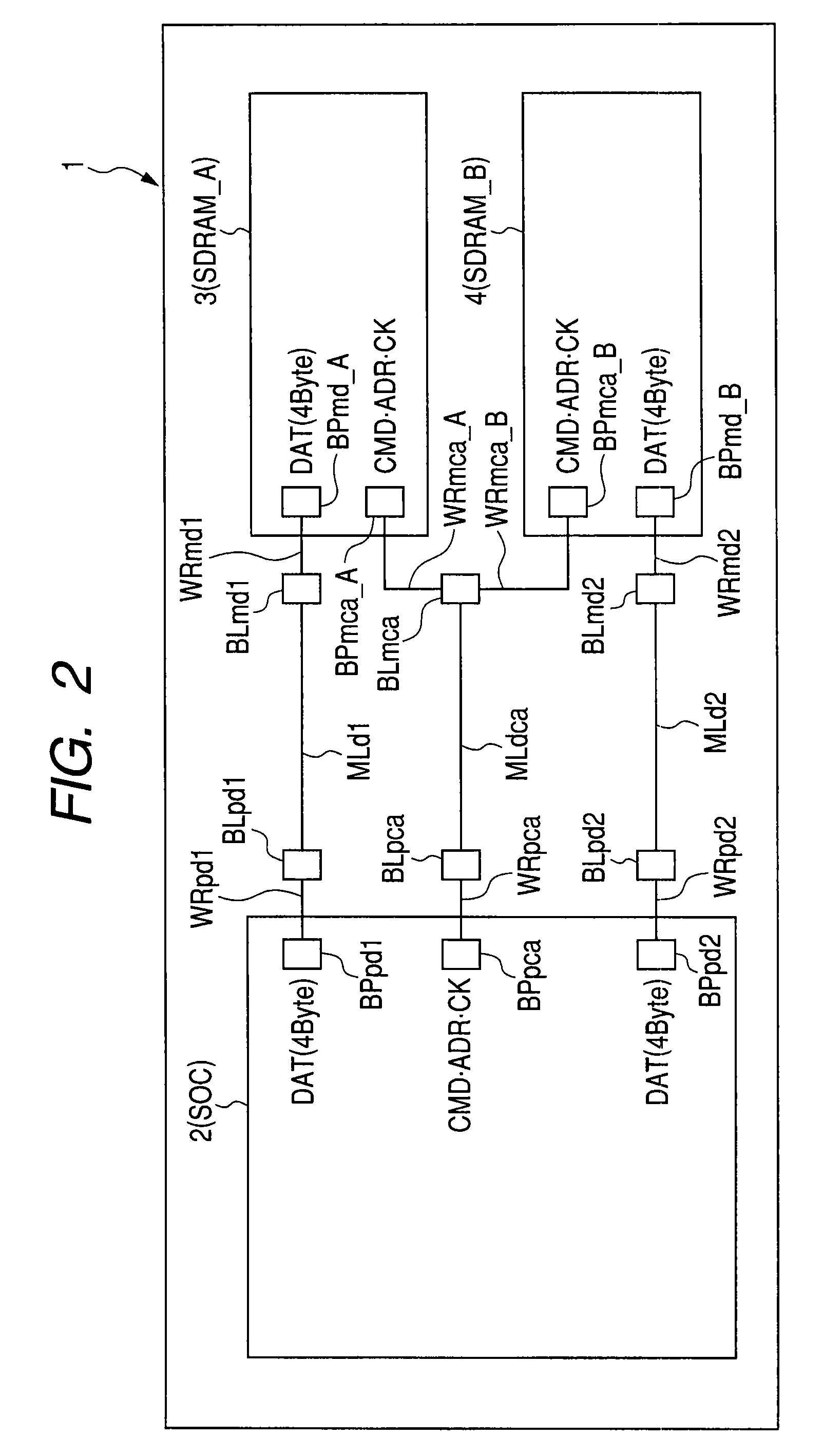
[0038]First, a typical embodiment of the invention disclosed in the present application will briefly be explained. Referential numerals with parentheses in the drawings to be referred to in the summary of the typical embodiment simply illustrate what are included in the concept of components to which they are attached.

[0039][1] A semiconductor device according to a typical embodiment of the present invention comprises, on its module board (5), a plurality of memory chips (3, 4) in a stacked state and a data processor chip (2) capable of simultaneously accessing the memory chips. A plurality of address system bonding pads (BPpca) related to an address and a command for the data processor chip to access the memory chip are connected, through a common address system wiring (MLca) among the memory chips, to address system bonding pads (BPmca_A, BPmca_B) to which the memory chips correspond. A plurality of data system bonding pads (BPpd1, BPpd2) related to data a...


PUM


Abstract

There is provided a semiconductor device which makes equalization of wirings between address system chips easy and reduce the influence of crosstalk noise and capacitive coupling noise among data system wirings for connecting the chips. There are mounted, on a module board, a plurality of stacked memory chips which a data processor chip simultaneously accesses. Address system bonding pads to which a plurality of memory chips correspond are commonly coupled by a wire to a bonding lead at one end of the module board wiring whose other end is coupled by a wire to an address system bonding pads of the data processor. Data system bonding pads of the data processor chip are individually coupled to data system bonding pads of the memory chip. With respect to an arrangement of the plurality of data system bonding pads of the data processor chip, an arrangement of the data system bonding pads to which the memory chip, coupled by the data system wiring, corresponds is made such that memory chips are disposed in an alternating sequence.

Description

CROSS-REFERENCE TO RELATED APPLICATIONS[0001]The disclosure of Japanese Patent Application No. 2007-92591 filed on Mar. 30, 2007 including the specification, drawings and abstract is incorporated herein by reference in its entirety.BACKGROUND OF THE INVENTION[0002]The present invention relates to a semiconductor device, such as an SIP (System In Package), wherein a memory chip and a data processor chip are mounted on a module board or substrate. In particular, it relates, for instance, to a technique effective to be applied to a resin-sealed semiconductor module of the SIP type.[0003]Described in Patent document 1 is a semiconductor module wherein there are mounted on a module board two DDR2-SDRAMs (Double Data Rate 2-Synchronous Dynamic Random Access Memory) and a data processor which lie flat, respectively. Layouts of data system terminals of the DDR2-SDRAMs with respect to memory access terminals of the data processor are determined in such a manner that wirings for data and a da...

Claims


Application Information

Patent Timeline
Patent Type & Authority Patents(United States)
IPC IPC(8): H01L23/50
CPCG11C5/02G11C5/04G11C5/063H01L23/50H01L23/5386H01L23/552H01L24/48H01L24/49H01L24/73H01L25/0652H01L25/18H01L2224/16H01L2224/32145H01L2224/48091H01L2224/48227H01L2224/48233H01L2224/48235H01L2224/49171H01L2224/49175H01L2224/73265H01L2225/0651H01L2225/06562H01L2924/00014H01L2924/01004H01L2924/01005H01L2924/01006H01L2924/01015H01L2924/01033H01L2924/01078H01L2924/01082H01L2924/014H01L2924/14H01L2924/15192H01L2924/15311H01L2924/181H01L2924/3025H01L2924/00H01L2924/00012H01L2224/32225H01L2224/45099H01L2224/05599
Inventor YOSHIKAWA, YASUHIROSUWA, MOTOOSAKATA, KAZUYUKI
Owner RENESAS ELECTRONICS CORP
Why Eureka
Try Eureka