

Method for manufacturing semiconductor device
a manufacturing method and semiconductor technology, applied in the direction of semiconductor devices, basic electric elements, electrical appliances, etc., can solve the problems of physical stress and degrade and achieve the effect of reducing physical stress and increasing the reliability of the semiconductor devi
- Summary
- Abstract
- Description
- Claims
- Application Information
AI Technical Summary
Benefits of technology
Problems solved by technology
Method used
Image

Examples
Embodiment Construction
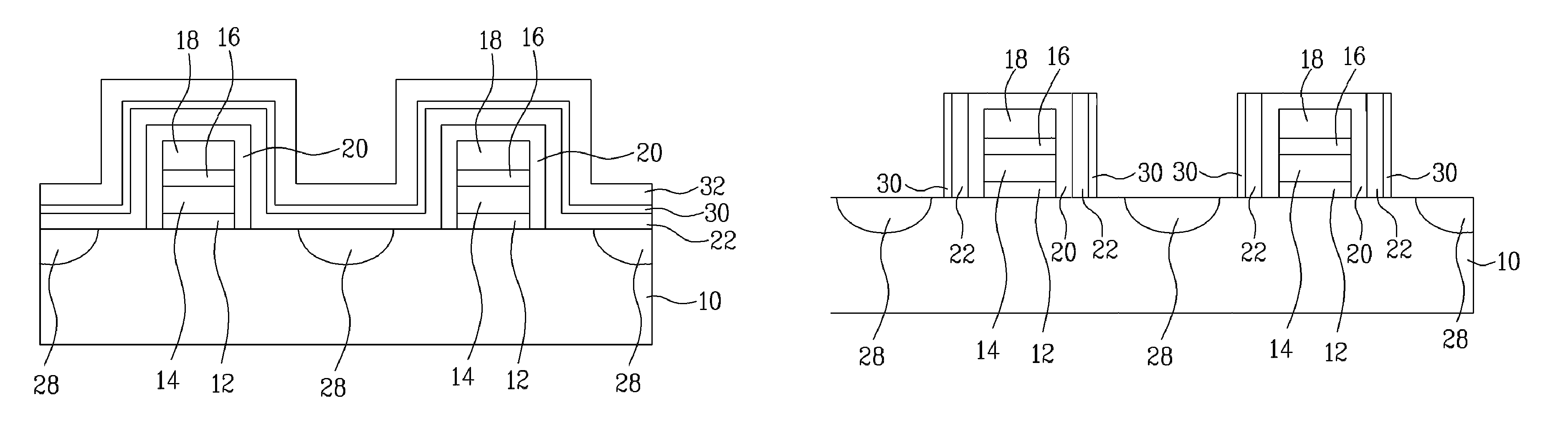
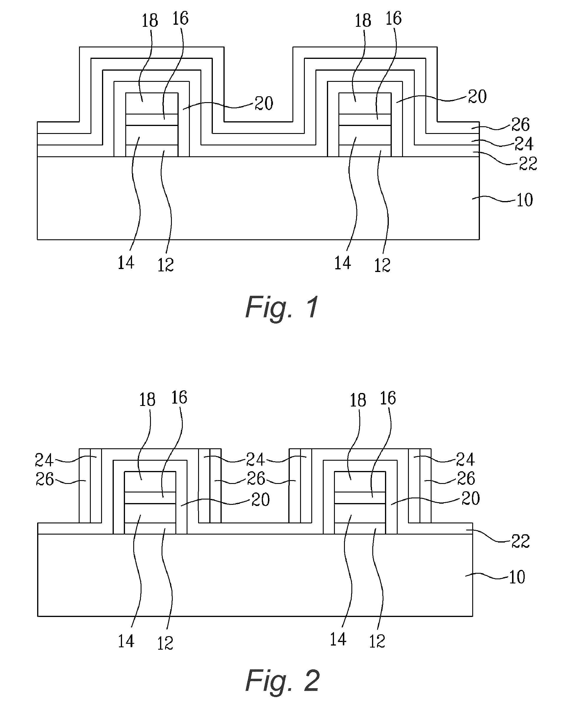
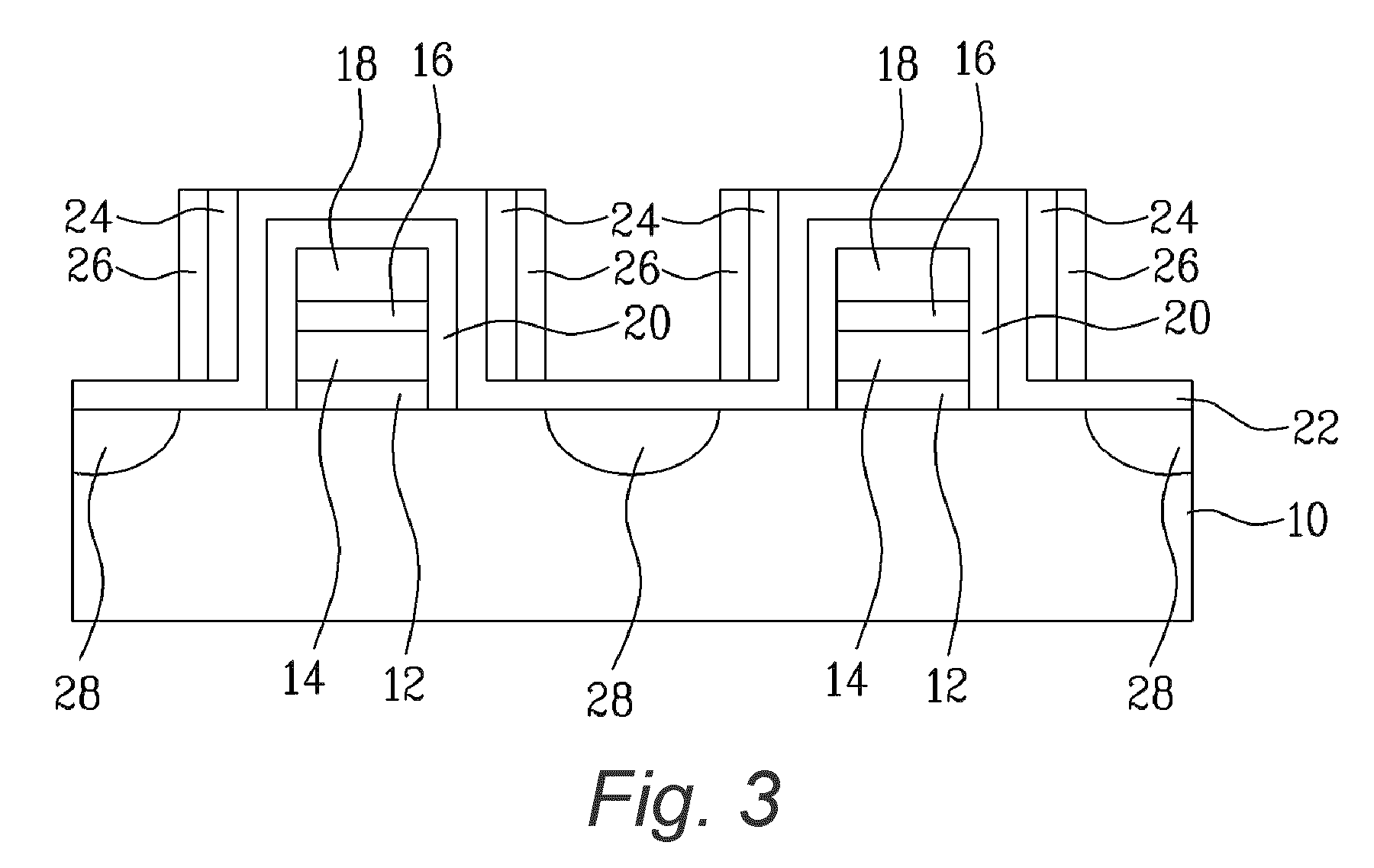
[0006]In general, example embodiments of the present invention relate to methods for manufacturing a semiconductor device. Some example embodiments of the invention may increase the reliability of the semiconductor device by reducing physical stress applied to a gate pattern of the device and thereby help to prevent the gate pattern from defining a trap.
[0007]In one example embodiment of the present invention, a method for manufacturing a semiconductor device includes various steps. First, a gate pattern is formed on a substrate. Next, a first oxide layer is formed on horizontal and vertical surfaces of the gate pattern. Then, a second oxide layer, a first silicon nitride layer, and a second silicon nitride layer are sequentially formed over exposed surfaces of the substrate and the first oxide layer. Next, a first etching process is performed to remove horizontal portions of the first and second silicon nitride layers such that only vertical portions of the first and second silicon...
PUM
| Property | Measurement | Unit |
|---|---|---|
| thickness | aaaaa | aaaaa |
| physical stress | aaaaa | aaaaa |
| electrical | aaaaa | aaaaa |
Abstract
Description
Claims
Application Information