Calibration circuit, semiconductor device including the same, and method of adjusting output characteristics of semiconductor device

a technology of calibration circuit and output buffer, which is applied in logic circuits, testing/calibration of speed/acceleration/shock measurement devices, and automatic control, etc. it can solve the problems of severe impedance impedance of output buffer, affecting the accuracy of output buffer impedance, etc., to achieve accurate calibration operation, increase data transfer speed on the system, and improve the effect of data processing system speed

Inactive Publication Date: 2010-07-13
LONGITUDE LICENSING LTD
View PDF19 Cites 26 Cited by
  • Summary
  • Abstract
  • Description
  • Claims
  • Application Information

AI Technical Summary

Benefits of technology

[0007]It is another object of the present invention to provide a method of adjusting output characteristics of a semiconductor device capable of accurately adjusting an impedance of the output buffer, based on the calibration operation.
[0019]As explained above, according to the present invention, the reference voltage can be adjusted. Therefore, the reference voltage can be offset by considering the resistance component present between the calibration terminal and the external terminal. Accordingly, the impedance of the replica buffer can be set to a value considering the resistance component on the package, and a more accurate calibration operation can be carried out.
[0020]Further, by carrying out the accurate calibration operation, the data transfer speed on the system can be increased, and a higher-speed data processing system can be configured.

Problems solved by technology

If the input / output signals have reduced amplitudes, the desired accuracy of impedances of output buffers becomes severe.
Also, during its actual use, the impedance of the output buffer is affected by variations in ambient temperature and power source voltage.

Method used


Image

  • Calibration circuit, semiconductor device including the same, and method of adjusting output characteristics of semiconductor device
  • Calibration circuit, semiconductor device including the same, and method of adjusting output characteristics of semiconductor device
  • Calibration circuit, semiconductor device including the same, and method of adjusting output characteristics of semiconductor device

Examples


Embodiment Construction

[0035]Preferred embodiments of the present invention will now be explained in detail with reference to the drawings.

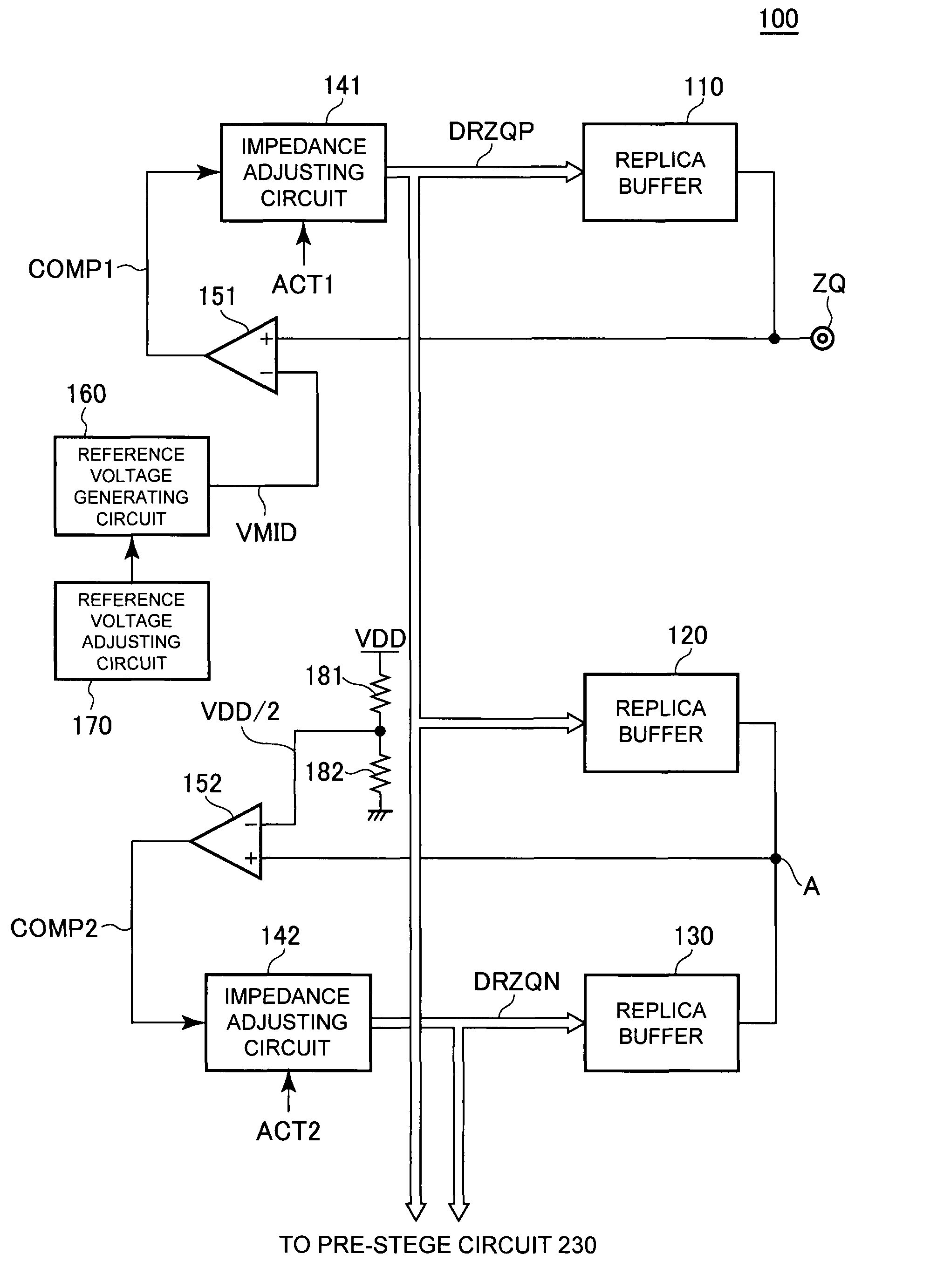
[0036]FIG. 1 is a circuit diagram of a calibration circuit 100 according to a preferred embodiment of the present invention.

[0037]As shown in FIG. 1, the calibration circuit 100 of the present embodiment includes replica buffers 110, 120, and 130, an impedance adjusting circuit 141 for controlling the impedances of the replica buffers 110 and 120, a impedance adjusting circuit 142 for controlling the impedance of the replica buffer 130, a comparator 151 for controlling the impedance adjusting circuit 141, and a comparator 152 for controlling the impedance adjusting circuit 142.

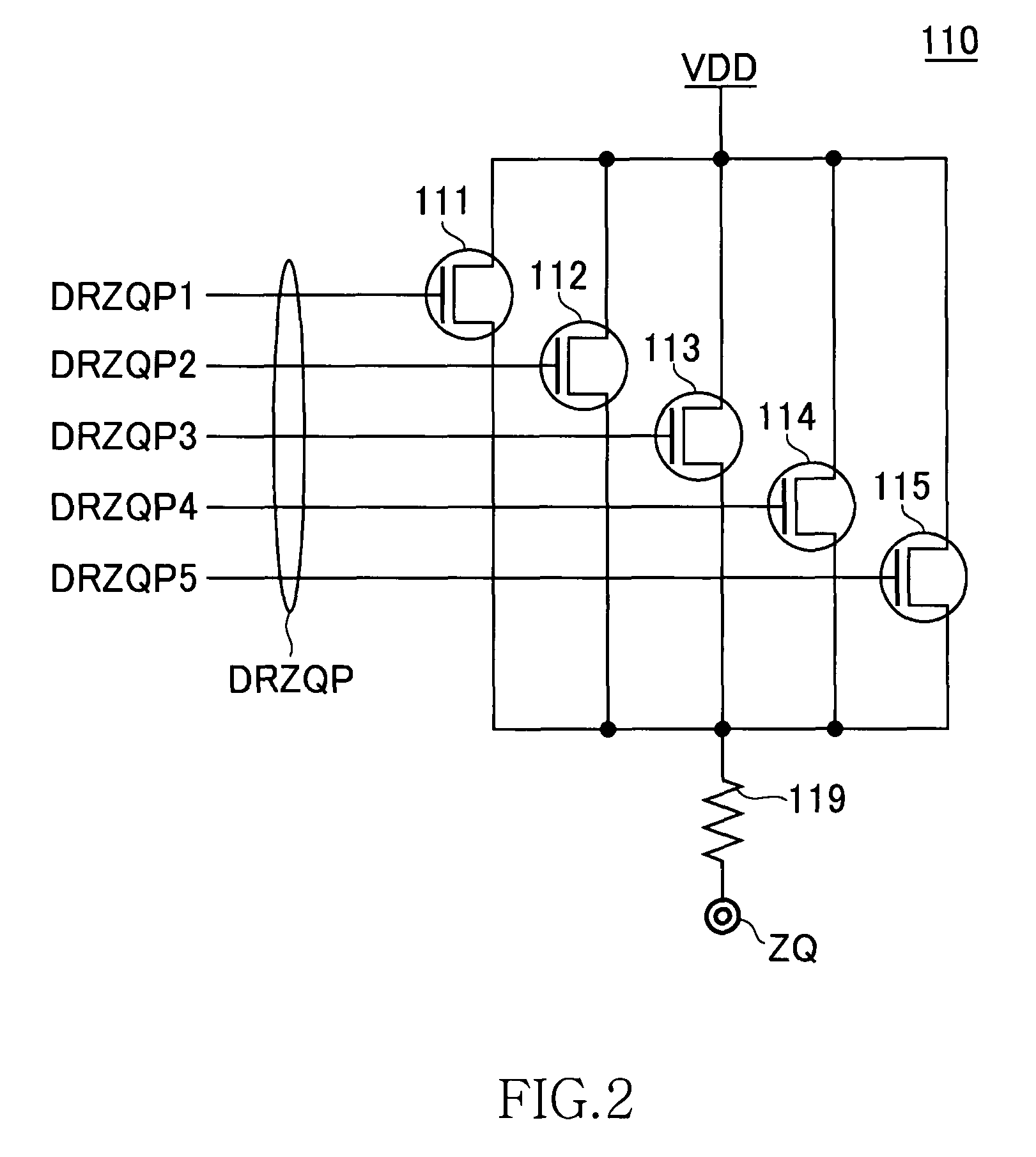
[0038]The replica buffers 110, 120, and 130 have the same circuit configuration as a part of an output buffer which will be described later. The output impedance is adjusted by using the replica buffers 110, 120, and 130 and the result is reflected in the output buffer. The impedance of the outpu...


PUM


Abstract

A calibration circuit includes: a replica buffer that drives a calibration terminal ZQ; a reference voltage generating circuit that generates a reference voltage VMID; a comparing circuit that compares a voltage appearing in the calibration terminal ZQ with the reference voltage VMID; an impedance adjusting circuit that changes an output impedance of the replica buffer based on a result of comparison carried out by the comparing circuit; and a reference voltage adjusting circuit that adjusts the reference voltage VMID. With this arrangement, the reference voltage VMID can be offset by taking into account a resistance component present between the calibration terminal ZQ and the external terminal, and therefore, a more accurate calibration operation can be carried out.

Description

TECHNICAL FIELD[0001]The present invention relates to a calibration circuit and a semiconductor device including the same, and, more particularly to a calibration circuit that adjusts an output impedance of an output buffer, and a semiconductor device including the calibration circuit. The present invention also relates to a method of adjusting output characteristics of a semiconductor device, and, more particularly to an output-characteristic adjusting method of adjusting an output impedance of an output buffer. The present invention also relates to a data processing system that includes a semiconductor memory device having a calibration circuit.BACKGROUND OF THE INVENTION[0002]In recent years, significantly high data transfer rate is required for data transfer between semiconductor devices (between CPUs and memories for example). To accomplish high data transfer rate, the amplitude of input / output signals is increasingly reduced. If the input / output signals have reduced amplitudes...

Claims


Application Information

Patent Timeline
Patent Type & Authority Patents(United States)
IPC IPC(8): G01R35/00G01D18/00
CPCH03K19/00384
Inventor HOSOE, YUKIKUROKI, KOJI
Owner LONGITUDE LICENSING LTD
Why Eureka
Try Eureka