Measurement board for electronic device test apparatus

a technology for electronic devices and test apparatus, applied in the direction of individual semiconductor device testing, coupling device connection, instruments, etc., can solve the problems of large signal loss and difficulty in securing stable transmission characteristics, and achieve the effect of convenient and inexpensive stabilization of transmission characteristics of measuremen

Active Publication Date: 2008-07-29
ADVANTEST CORP
View PDF5 Cites 11 Cited by
  • Summary
  • Abstract
  • Description
  • Claims
  • Application Information

AI Technical Summary

Benefits of technology

[0010]An object of the present invention is to provide a measurement board, performance board, and probe card able to secure stable transmission characteristics with low loss and low reflection and suppress the leakage of the signal to the outside and the entry of noise even when using a high frequency signal to test an electronic device under test.
[0012]In the present invention, at least part of the front exposed part of the center contact of the coaxial connector passing through the base board is covered by the cover member to correct the impedance of the front exposed part. Due to this, the impedance of the front exposed part of the center contact can be matched with the surrounding impedance, so low loss, low reflection, stabilized transmission characteristics can be secured.
[0013]Further, since the bent front exposed part is covered by the cover member, it is possible to suppress leakage of the signal from the front exposed part to the outside and entry of noise through the front exposed part to the transmission line.
[0018]By alternately stacking, in addition to the first dielectric and first conductor interconnect, a plurality of second dielectrics and second conductor interconnects, the cover member is increased in thickness, so attachment of the cover member to the base board becomes easier. Further, by electrically connecting the first conductor interconnect and the plurality of second conductor interconnects through the via holes, the first conductor interconnect can be reliably connected to the GND of the coaxial connector or the GND layer of the base board.
[0020]In the above invention, while not particularly limited to this, preferably the surface of the cover member to be soldered to the base board has a metal plating layer. Due to this, the cover member can be easily attached to the base board.
[0024]By later attaching the cover member to the front exposed part of the center contact of the coaxial connector, it becomes possible to easily and inexpensively stabilize the transmission characteristics of a measurement board to which a through-the-board type of coaxial connector is already attached.

Problems solved by technology

In particular, in a test of an IC device performed using a high frequency signal of for example several GHz or more, there is large signal loss and reflection at the front exposed part 51a where the impedance mismatch occurs, so there is the problem that securing stable transmission characteristics is difficult.

Method used


Image

  • Measurement board for electronic device test apparatus
  • Measurement board for electronic device test apparatus
  • Measurement board for electronic device test apparatus

Examples


second embodiment

[0053]FIG. 4A is a perspective view of a cover member according to a second embodiment of the present invention, while FIG. 4B is a cross-sectional view along the line IVB-IVB of FIG. 4A.

[0054]The performance board according to the present embodiment differs from the first embodiment in the point of differing in thickness of the cover member 80A, but the rest of the configuration is the same. Below, only the point of difference of the performance board in the present embodiment from the first embodiment will be explained.

[0055]The cover member 80B in the present embodiment, as shown in FIG. 4A and FIG. 4B, is provided with, in addition to the first board 81 and first GND layer 82, two second boards 83 and two second GND layers 84.

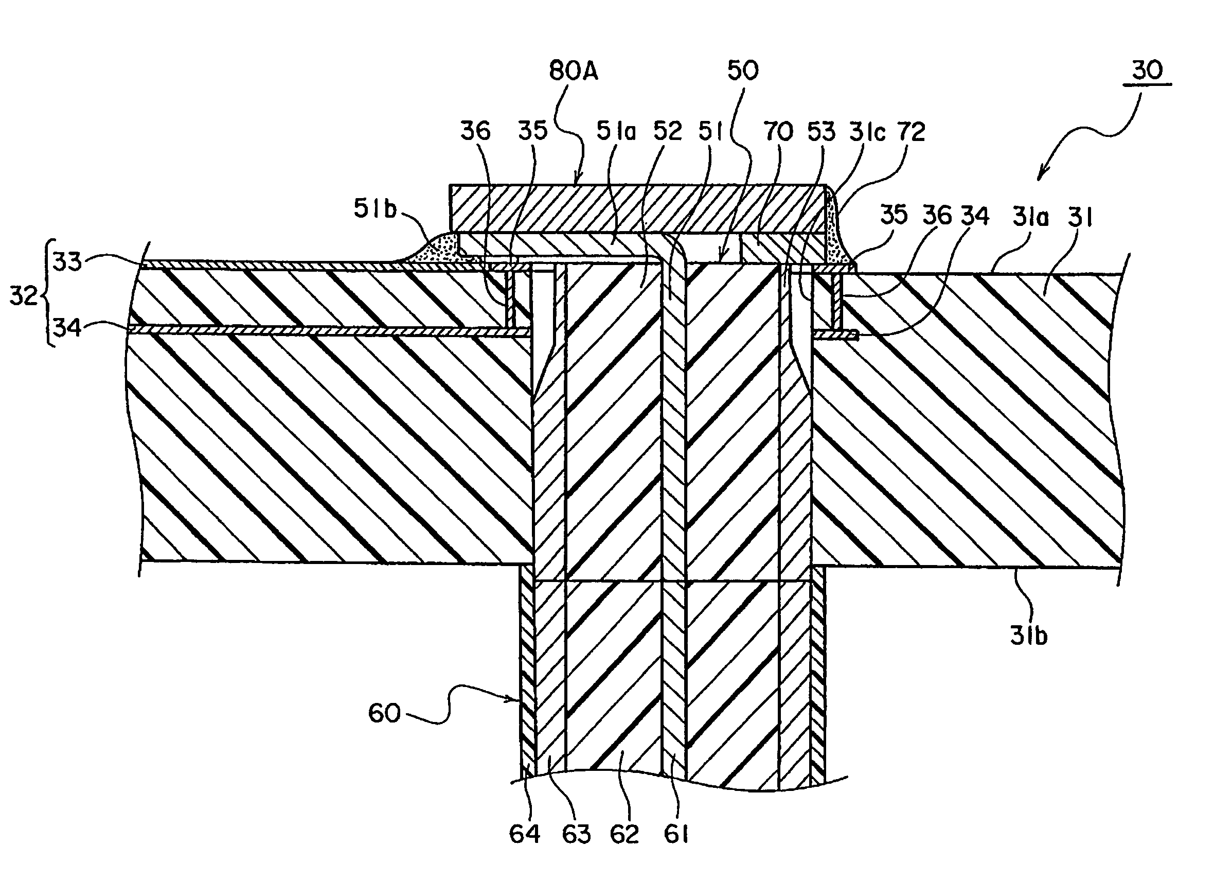
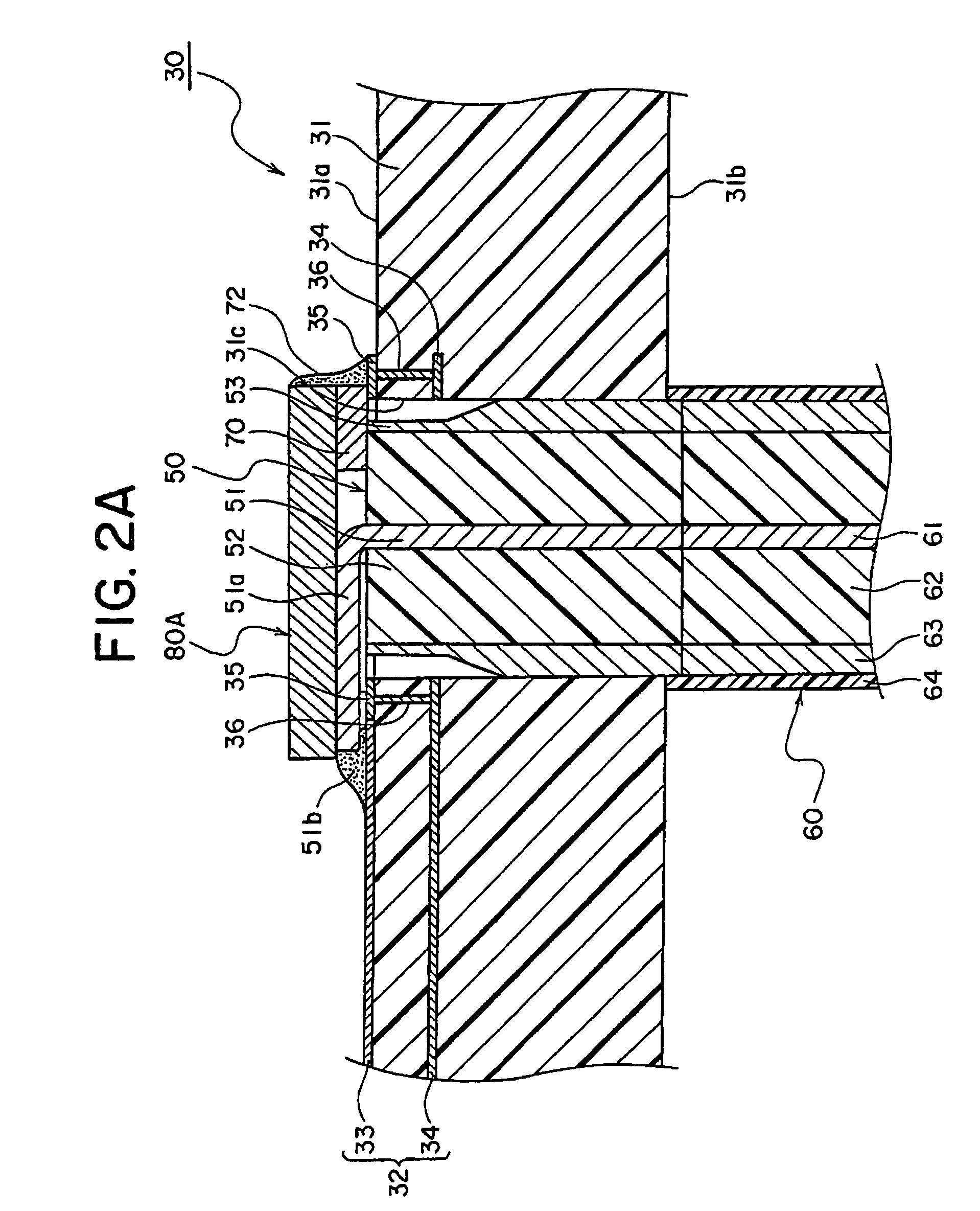
[0056]The first board 81, in the same way as the first cover member 80A, is arranged so as to contact the front exposed part 51a of the center contact 51 of the coaxial connector 50 (shown by the broken line in FIG. 4B) through the signal pattern 87. Furthe...

third embodiment

[0063]FIG. 5 is an enlarged sectional view showing the connection part of the coaxial connector in the performance board according to a third embodiment of the present invention.

[0064]In the first and second embodiments, the explanation was given of covering only a single coaxial connector 50 passing through the through hole 31a (specifically the front exposed part 51a of the center contact 51) by the cover members 80A and 80B, but as shown in FIG. 5, it is also possible to cover a plurality of coaxial connectors 50 connected by the same signal pattern 33 on the base board 31 by a single cover member 80C.

[0065]In the first to third embodiments, the explanation was given of an example of application of the present invention to a performance board used for the test of a packaged IC device. While the present invention is not particularly limited to this, as explained in the following fourth embodiment, it is also possible to apply the invention to a probe card used for the test of an I...

fourth embodiment

[0066]FIG. 6 is a cross-sectional view showing a probe card according to a fourth embodiment of the present invention.

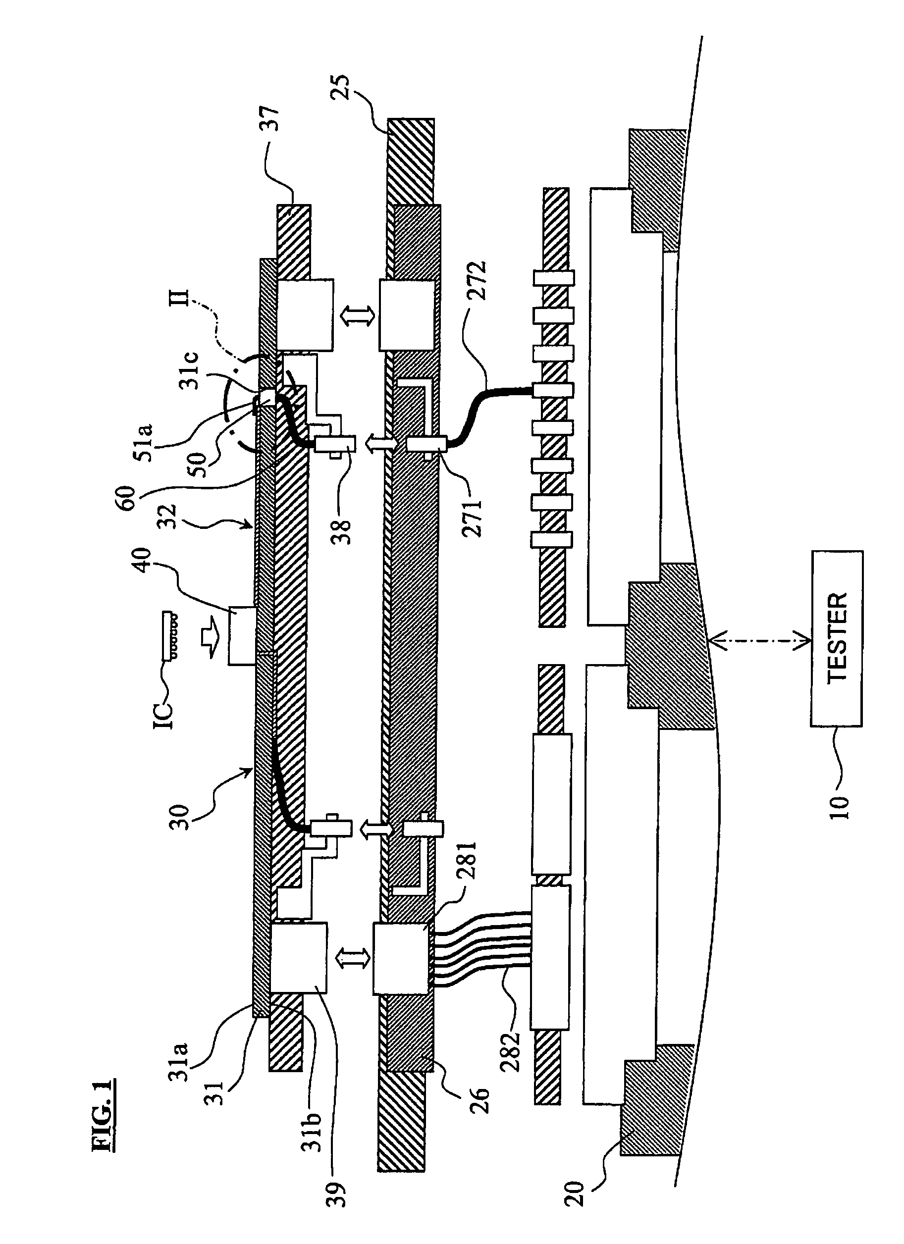
[0067]The probe card 90 according to the present embodiment, as shown in FIG. 6, is provided with a plurality of probe needles 91 for electrical connection to an IC device, a base board 92 to which the probe needles 91 are mounted on the front surface 92a, a coaxial connector 95 inserted in a through hole 92c from the back surface 92b toward the front surface 92a of the base board 92, and a stiffener 94 attached to the back surface 92b of the base board 92 for improving the structural strength of the probe card 90. The front exposed part 95a of the center contact of the coaxial connector 95 is electrically connected to a signal pattern 93 formed on the front surface 92a of the base board 92.

[0068]While the illustration is omitted in FIG. 6, in the present embodiment, the front exposed part 95a of the coaxial connector 95 is covered by a cover member 80A in the same w...


PUM


Abstract

A performance board able to secure low loss, low reflection, stable transmission characteristics even when using a high frequency signal to test an electronic device and able to suppress signal leakage to the outside and entry of noise, provided with a base board having a signal pattern electrically connected with a socket formed on its front surface, a coaxial connector to which a coaxial cable electrically connecting the performance board and test apparatus is connected, passing through the base board from the back surface toward the front surface, and having a front exposed part of the center contact bent and electrically connected to the signal pattern, and a cover member covering the front exposed part of the center contact and correcting the impedance of the front exposed part.

Description

BACKGROUND OF THE INVENTION[0001]1. Field of the Invention[0002]The present invention relates to a measurement board, performance board, and probe card for electrically connecting an IC device and a test apparatus when testing a semiconductor integrated circuit device or other various types of electronic devices (hereinafter also referred to representatively as “IC devices”) by a test apparatus.[0003]2. Description of the Related Art[0004]In the process of production of an IC device or other electronic device, an electronic device test apparatus is used for testing the performance and functions of the IC device in the packaged state.[0005]This electronic device test apparatus is provided with a performance board with a socket attached to its front surface and connected to a test head via a coaxial cable and tests an IC device by the transfer of test signals between an IC device electrically connected to the socket and the tester.[0006]Above this performance board, a handler for tran...

Claims


Application Information

Patent Timeline
Patent Type & Authority Patents(United States)
IPC IPC(8): G01R31/02
CPCG01R1/0408H01R24/52H01R2103/00
Inventor MINEO, HIROYUKISHIBUYA, ATSUNORI
Owner ADVANTEST CORP
Why Eureka
Try Eureka