

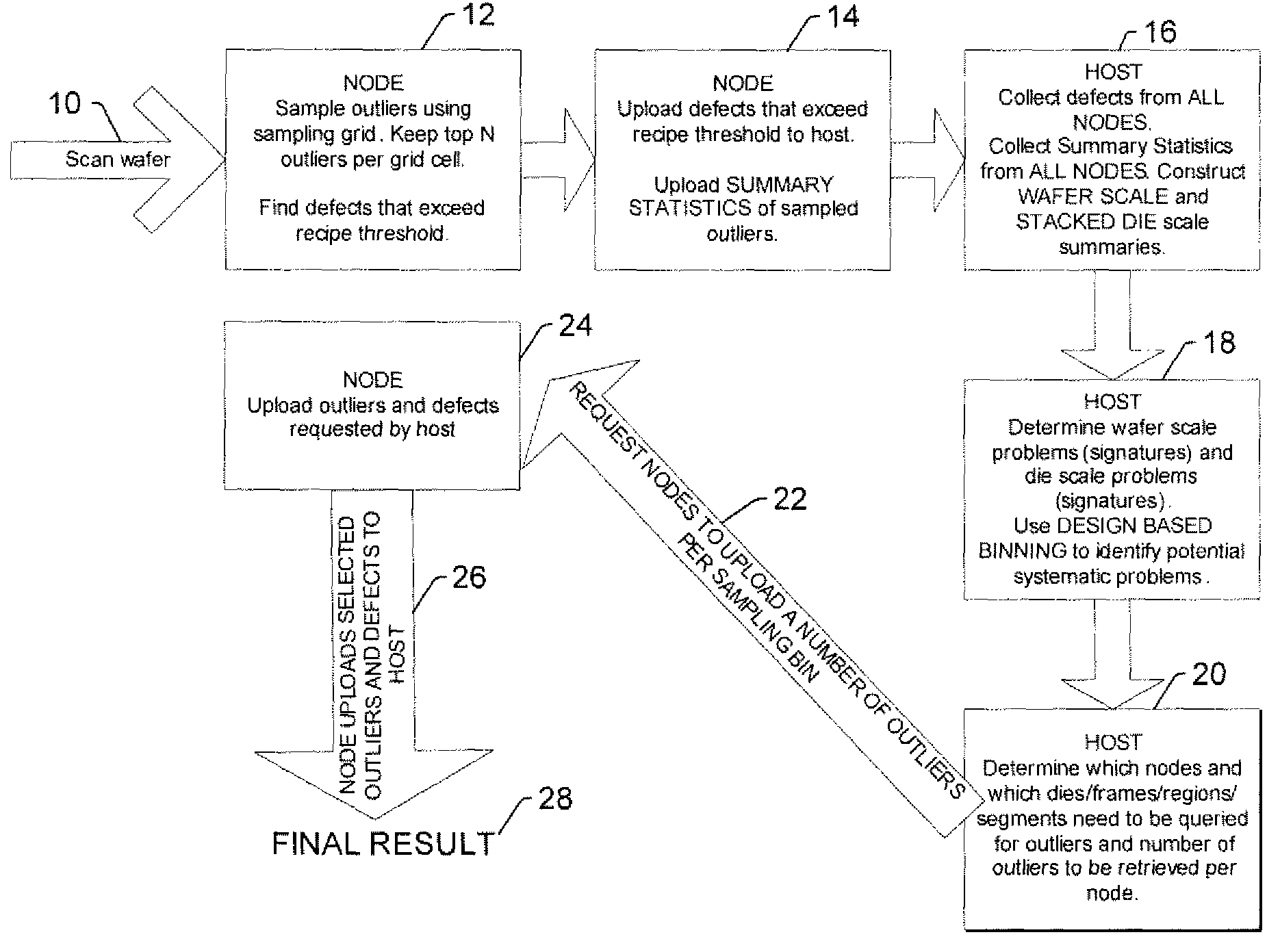
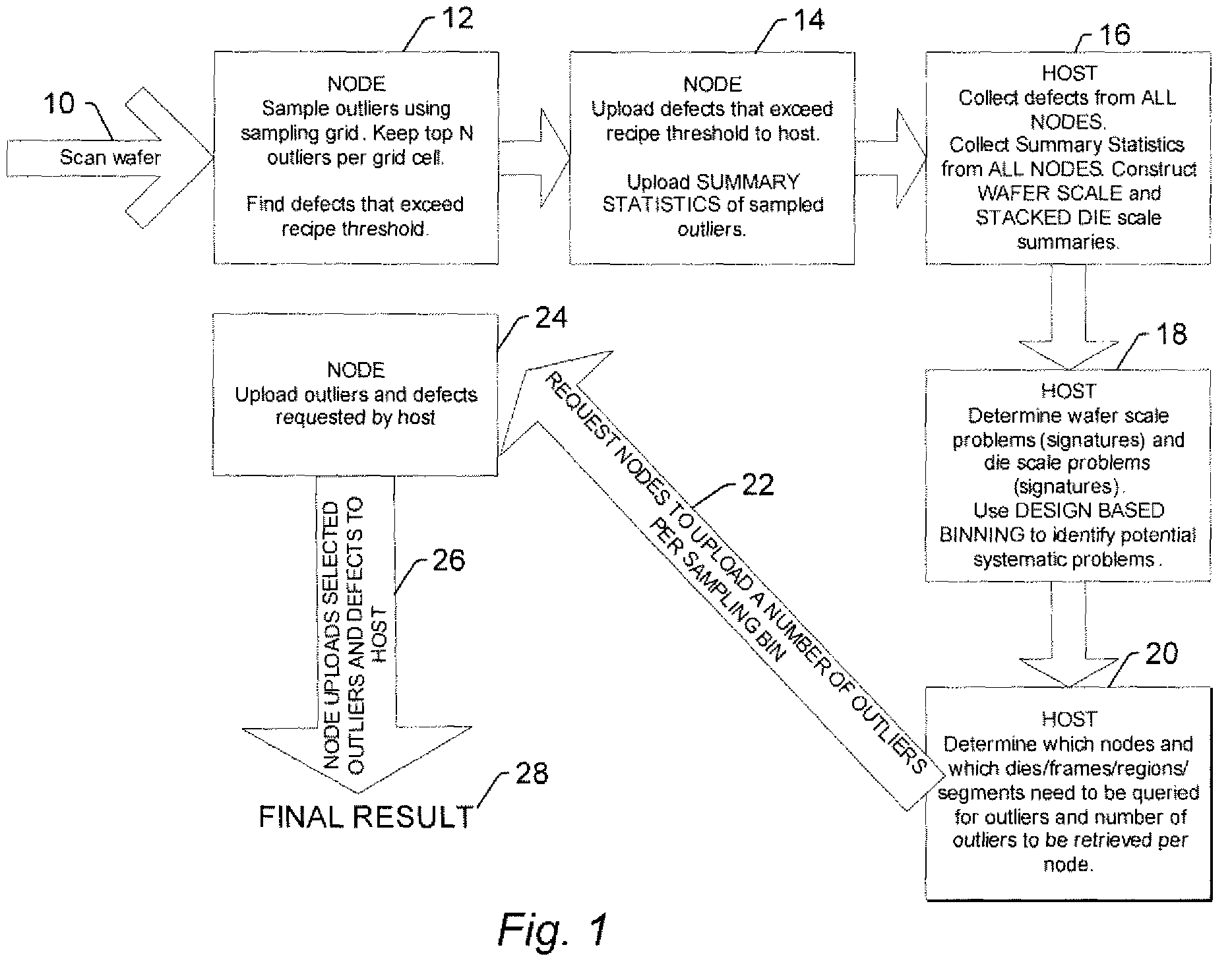
Systems and methods for detecting defects on a wafer and generating inspection results for the wafer
a technology of system and method, applied in the direction of total factory control, programme control, instruments, etc., can solve the problems of not using global, i.e., wafer wide criteria, to determine the defects to be reported (or not), and not simultaneously sampling random and systematic defects
- Summary
- Abstract
- Description
- Claims
- Application Information
AI Technical Summary
Benefits of technology
Problems solved by technology
Method used
Image

Examples
Embodiment Construction
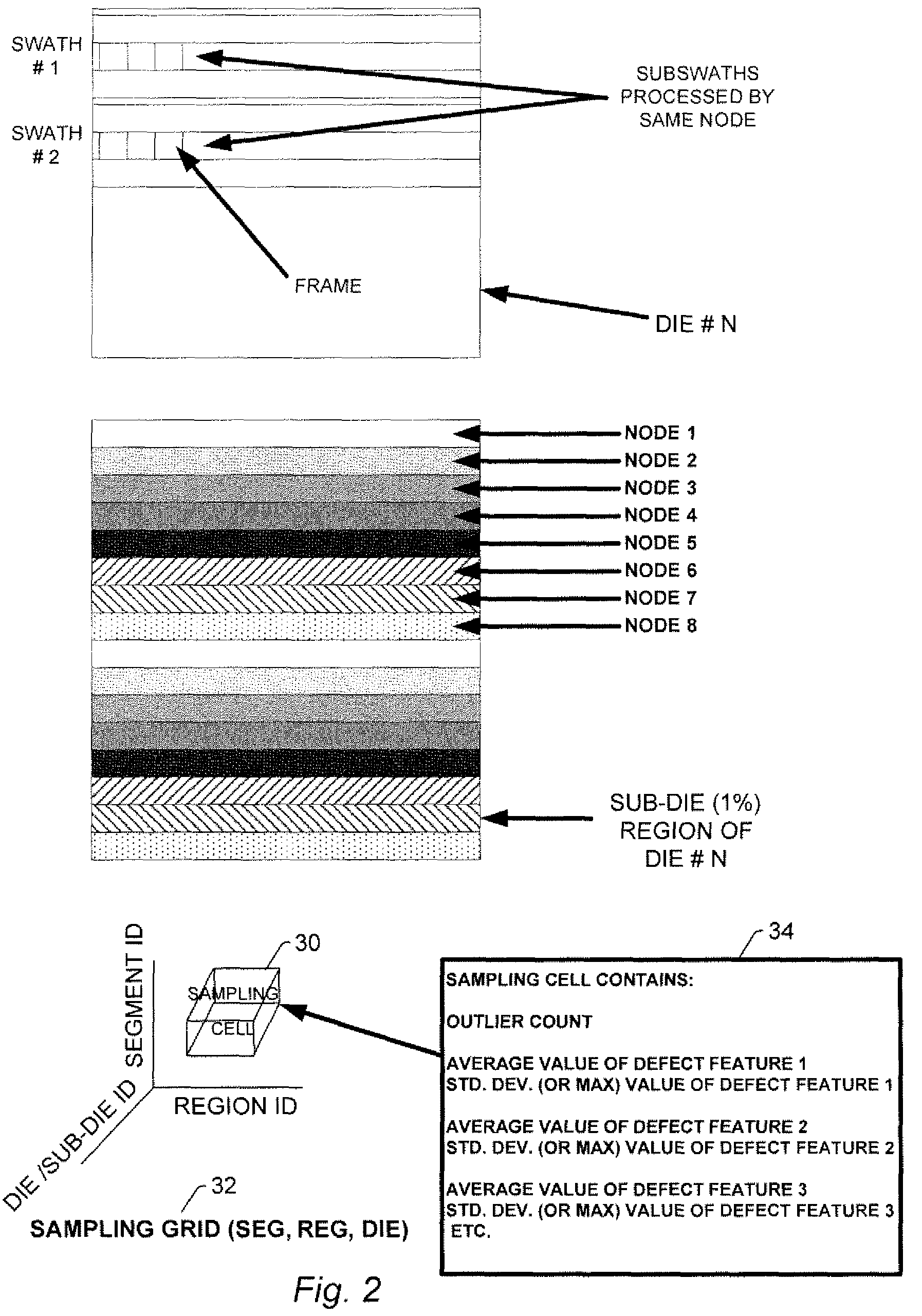
[0028]As used herein, the term “wafer” generally refers to substrates formed of a semiconductor or non-semiconductor material. Examples of such a semiconductor or non-semiconductor material include, but are not limited to, monocrystalline silicon, gallium arsenide, and indium phosphide. Such substrates may be commonly found and / or processed in semiconductor fabrication facilities.
[0029]One or more layers may be formed upon a wafer. Many different types of such layers are known in the art, and the term wafer as used herein is intended to encompass a wafer on which all types of such layers may be formed. One or more layers formed on a wafer may be patterned. For example, a wafer may include a plurality of dies, each having repeatable patterned features. Formation and processing of such layers of material may ultimately result in completed semiconductor devices. As such, a wafer may include a substrate on which not all layers of a complete semiconductor device have been formed or a sub...
PUM
| Property | Measurement | Unit |
|---|---|---|
| defect detection thresholds | aaaaa | aaaaa |
| defect detection threshold | aaaaa | aaaaa |
| defects | aaaaa | aaaaa |
Abstract
Description
Claims
Application Information