Method and apparatus for storing and distributing memory repair information

a technology of memory repair and information storage, applied in the field of integrated circuits, can solve the problems of processing overload, inability to support memory incorporating a mixture of parallel and serial repair approaches, and adversely affecting the ability of the integrated circuit housing them to operate in its intended manner

Active Publication Date: 2010-07-13
SIEMENS PROD LIFECYCLE MANAGEMENT SOFTWARE INC
View PDF14 Cites 70 Cited by
  • Summary
  • Abstract
  • Description
  • Claims
  • Application Information

AI Technical Summary

Benefits of technology

[0034]The fuse box interface facilitates the integration of different non-volatile memories as fuse boxes while presenting a fixed interface to the fuse box controller.
[0035]The fuse box controller contains no memory-specific information. Rather it self-discovers the length of the chain formed by the BISR registers, rendering it insensitive to the number, size and configuration of embedded memories and easily accommodating last-minute design changes to the number of memories, their order in the repair chain and their hierarchical order, if any, as a (nested) component of a pre-designed circuit block.
[0037]Further, the fuse box controller may implement a high order compression scheme to reduce the size of the central fuse box. The presence of the fuse box controller may obviate the communication of considerable amounts of repair data to an off-chip tester during a testing phase and processing of this data by the tester, in the form of compression and / or writing of repair information to the fuse box, which would otherwise be the case in its absence.
[0038]Repair data may be circulated along the daisy chain immediately upon initiation of the self-discovery process, thus considerably speeding up the repair process.

Problems solved by technology

During the manufacturing process, one or more of such memories will exhibit failures that may adversely impact the ability of the integrated circuit housing them to operate in its intended manner.
However, there have been a number of attempts at developing a centralized memory repair system, in part because generally only a small subset of a memory and only a small number of memories (on the order of 10) located on an integrated circuit will fail.
Moreover, they are unable to support memories incorporating a mixture of parallel and serial repair approaches.
Further, during testing of a plurality of integrated circuits on a single wafer to identify faults in the memories embedded therein, a considerable amount of information may be delivered to the tester in parallel causing a processing overload.
While Adams et at provides an on-chip controller to reduce the amount of information presented to an off-chip tester during a testing phase and introduces a fuse data compression scheme, the disclosed system remains specific to the number, size and configuration of the embedded memory locations and incapable of supporting memories incorporating a mixture of parallel and serial repair approaches.
While Puri1 discloses a fuse data compression scheme, the disclosed system remains specific to the number, size and configuration of the embedded memory locations and incapable of supporting memories incorporating a mixture of parallel and serial repair approaches.
Further, it provides no relief to an off-chip tester from information overload during a testing phase.
While Puri2 incorporates a central / shared fuse box concept, it does not disclose a fuse data compression scheme, the disclosed system remains specific to the number, size and configuration of the embedded memory locations and incapable of supporting memories incorporating a mixture of parallel and serial repair approaches and provides no relief to an off-chip tester from information overload during a testing phase.
While Tran et al use a shared fuse box architecture, they do not disclose a fuse data compression scheme, the disclosed system remains specific to the number, size and configuration of the embedded memory locations and incapable of supporting memories incorporating a mixture of parallel and serial repair approaches and provides no relief to an off-chip tester from information overload during a testing phase.
Nevertheless, Zappa et al do not disclose a fuse data compression scheme and the disclosed system remains specific to the number, size and configuration of the embedded memory locations and incapable of supporting memories incorporating a mixture of parallel and serial repair approaches and provides no relief to an off-chip tester from information overload during a testing phase.

Method used


Image

  • Method and apparatus for storing and distributing memory repair information
  • Method and apparatus for storing and distributing memory repair information
  • Method and apparatus for storing and distributing memory repair information

Examples


Embodiment Construction

[0059]The present invention will now be described for the purposes of illustration only, in conjunction with certain embodiments. It is to be understood that other objects and advantages of the present invention will be made apparent by the following description of the drawings according to the present invention.

[0060]While a preferred embodiment is disclosed, this is not intended to be limiting. Rather, the general principles set forth herein are considered to be merely illustrative of the scope of the present invention and it is to be further understood that numerous changes may be made without straying from the scope of the present invention. In particular, all dimensions described herein are intended solely to be exemplary for purposes of illustrating certain embodiments and are not intended to limit the scope of the invention to any embodiments that may depart from such dimensions as may be specified.

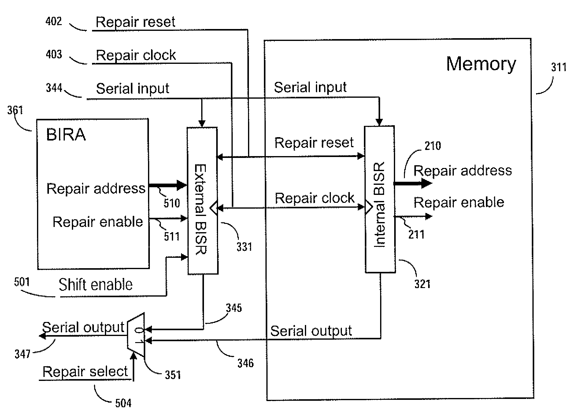
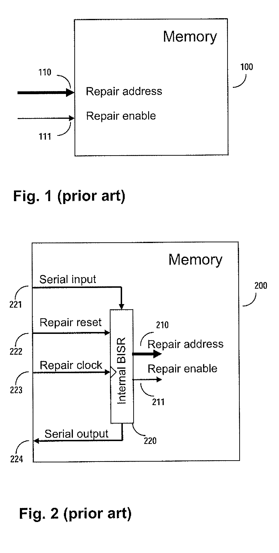
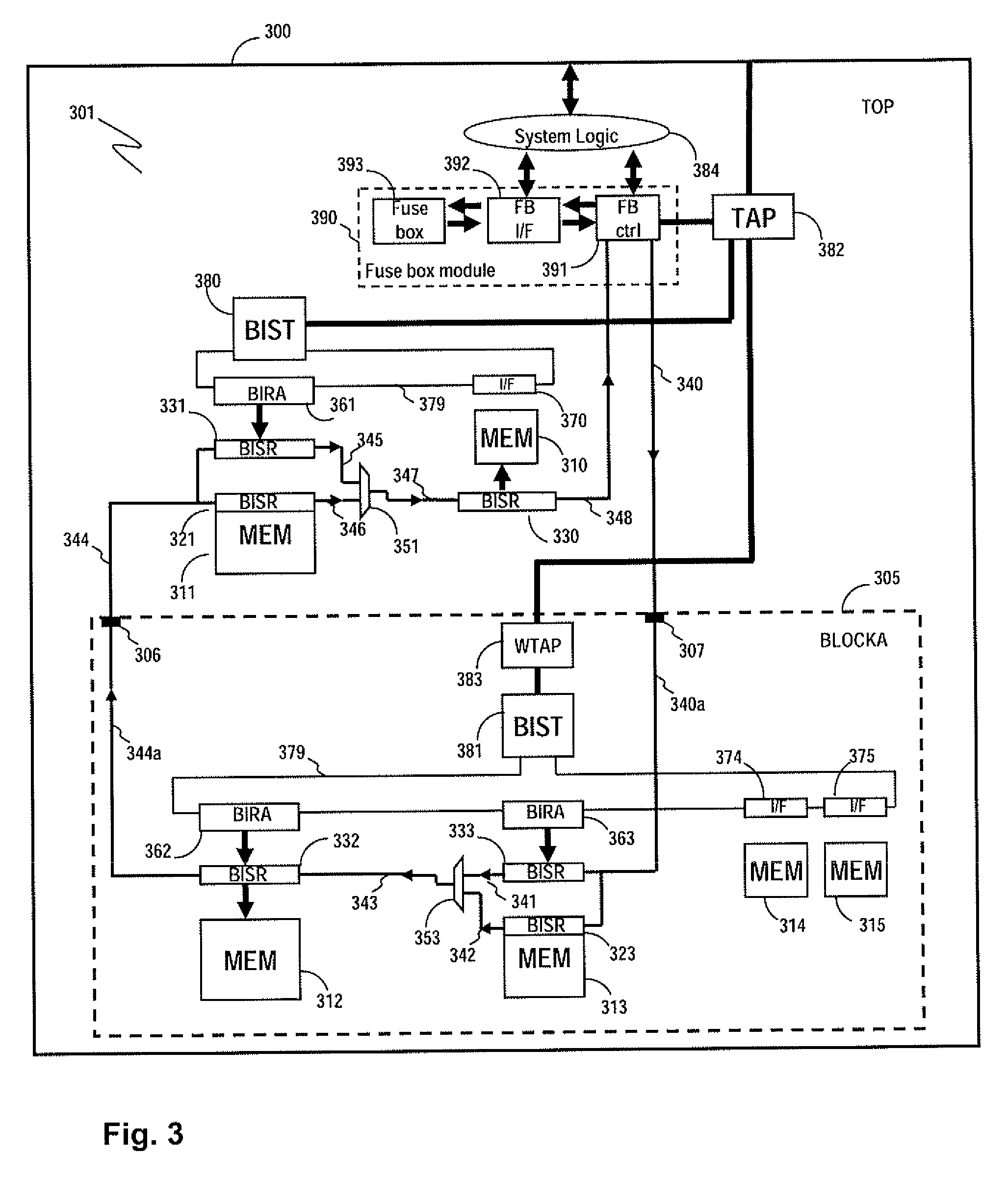
[0061]Referring first to FIG. 3, there is shown, an exemplary embodiment of th...


PUM


Abstract

A system for repairing embedded memories on an integrated circuit includes an external Built-In Self-repair Register (BISR) associated with every reparable memory. Each BISR is serially configured in a daisy chain with a fuse box controller. The controller determines the daisy chain length upon power up. The controller may perform a corresponding number of shift operations to move repair data between BISRs and a fuse box. Memories can have a parallel or serial repair interface. The BISRs may have a repair analysis facility into which fuse data may be dumped and uploaded to the fuse box or downloaded to repair the memory. Pre-designed circuit blocks provide daisy chain inputs and access ports to effect the system or to bypass the circuit block.

Description

RELATED APPLICATIONS[0001]The present invention claims priority from U.S. provisional Patent Application No. 60 / 825,185, which is incorporated herein by reference.FIELD OF THE INVENTION[0002]The present invention relates to integrated circuits, and more particularly to an innovative system for storing and distributing memory repair information on an integrated circuit.BACKGROUND OF THE INVENTION[0003]Integrated circuits may contain tens or even hundreds of embedded memories in conjunction with other circuitry. During the manufacturing process, one or more of such memories will exhibit failures that may adversely impact the ability of the integrated circuit housing them to operate in its intended manner.[0004]In order to increase yields of such integrated circuits, a large plurality of which may be found on a single integrated circuit wafer, a number memory repair techniques have been developed.[0005]Typically such techniques involve designing within each memory circuit, a plurality ...

Claims


Application Information

Patent Timeline
Patent Type & Authority Patents(United States)
IPC IPC(8): G11C29/00G01R31/28
CPCG11C29/4401G11C29/802G11C2029/0401G11C2229/726G11C2029/4402
Inventor NADEAU-DOSTIE, BENOITCOTE, JEAN-FRANCOIS
Owner SIEMENS PROD LIFECYCLE MANAGEMENT SOFTWARE INC
Why Eureka
Try Eureka