Process for fabricating semiconductor device

a technology of semiconductor devices and manufacturing processes, applied in the direction of semiconductor devices, electrical equipment, transistors, etc., can solve the problems of difficult use of glass substrates, inability to use large-area substrates, disadvantageous electrical characteristics of amorphous silicon films, etc., to reduce defects within films, increase crystallization, and reduce the effect of defects

Inactive Publication Date: 2010-08-03
SEMICON ENERGY LAB CO LTD
View PDF49 Cites 3 Cited by
  • Summary
  • Abstract
  • Description
  • Claims
  • Application Information

AI Technical Summary

Benefits of technology

[0035]The catalyst element for accelerating the crystallization can be introduced most effectively by coating the surface of the amorphous silicon film with a solution containing the catalyst element.
[0073]The defects that are present in the film cannot be reduced by irradiating a laser beam. Moreover, a laser beam irradiated to the surface of a silicon film brings about instantaneously a molten state as to generate a stress inside the film. The stress newly induces a defect. Accordingly, by applying heat treatment to the film, the stress can be relaxed to reduce the defects, and thereby a crystalline silicon film having excellent electrical characteristics can be obtained.

Problems solved by technology

However, the electric characteristics of the amorphous silicon film are disadvantageously poor.
However, the heat treatment for the crystallization of the amorphous silicon film requires heating the film at a temperature of 600° C. or higher for 20 hours or longer.
Such a heat treatment has a problem that it is difficult to use a glass as a substrate.
For instance, a Corning 7059 glass commonly used for the substrate of active matrix liquid crystal display devices has a glass deformation temperature of 593° C., and is therefore not suitable for using in large area substrates that are subjected to heating at a temperature of 600° C. or higher.
Accordingly, it is not possible to crystallize the film locally, or to control the crystallinity of a particular region.
That is, the method using Al or Sn is none the better as compared with the conventional crystallization of simply heating the amorphous silicon film.
If the elements are introduced insufficiently, the addition of the elements results in a small effect.
A film with favorable crystallinity cannot be expected in such a case.
If the elements are introduced in an excessive quantity, on the other hand, the semiconductive characteristics of silicon would be impaired.
It can be found from the above findings that not all nickel introduced by plasma treatment function sufficiently effective.
That is, even if nickel is introduced in a large quantity, it does not follow that all the nickel atoms function sufficiently.
However, vapor deposition is inferior concerning its controllability, and it fails to precisely control the quantity of catalyst element to be introduced in the amorphous silicon film.
However, there is still a problem that the crystallinity becomes an impurity.

Method used


Image

  • Process for fabricating semiconductor device
  • Process for fabricating semiconductor device
  • Process for fabricating semiconductor device

Examples


example 1

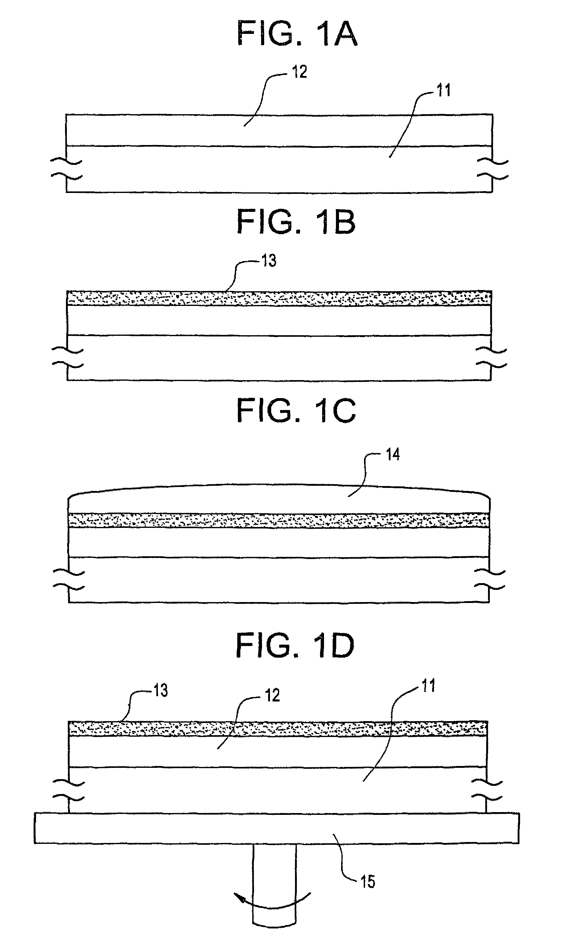
[0084]The present example refers to a process which comprises coating an amorphous silicon film with an aqueous solution containing a catalyst element for accelerating the crystallization of the film, and then irradiating a laser beam to increase the crystallinity of the crystallized film.

[0085]Referring to FIGS. 1(A) to 1(D), the process for introducing a catalyst element (nickel in this case) into the amorphous silicon film is described below. A Corning 7059 glass substrate having 100 mm×100 mm in size is used.

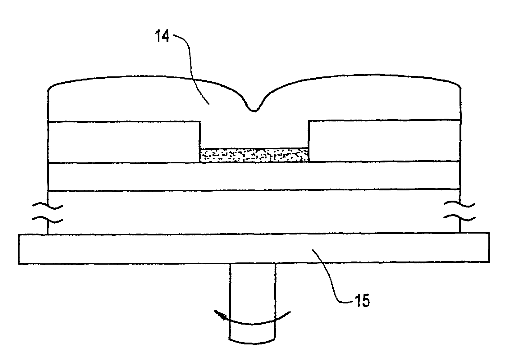
[0086]First, an amorphous silicon film of from 100 to 1,500 Å in thickness is deposited by plasma CVD or LPCVD. More specifically in this case, an amorphous silicon film 12 is deposited by plasma CVD at a thickness of 1,000 Å. (FIG. 1(A))

[0087]The resulting structure is subjected to a treatment using hydrofluoric acid to remove stains and natural oxide film, and an oxide film 13 is deposited thereafter to a thickness in a range of from 10 to 50 Å. In case stains are negligib...

example 2

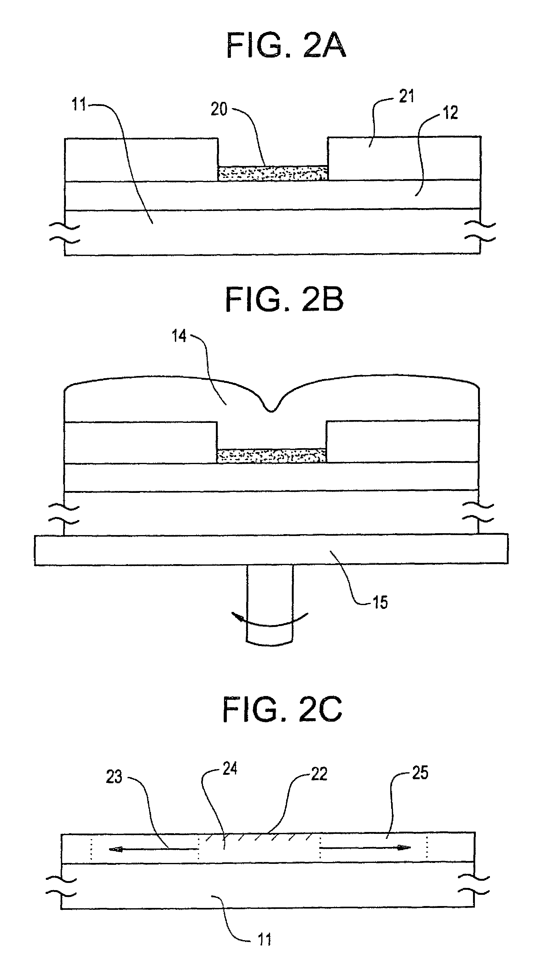
[0099]The present example refers to a fabrication process according to Example 1, which comprises fabricating a 1,200 Å thick silicon oxide film, and then introducing nickel selectively by using the silicon oxide film as a mask.

[0100]Referring to FIGS. 2(A) to 2(C), the process for fabricating a semiconductor device according to the present example is described below. A silicon oxide film 21 which functions as a mask is deposited of a thickness of 1,000 Å or more, more specifically in this case, at a thickness of 1,200 Å, on a Corning 7059 glass substrate (10 cm×10 cm in size). Considering the thickness of the silicon oxide film 21, however, it is found by the experiments of the present inventors that a film deposited at a thickness of 500 Å can be used without any problem so long as the film is deposited densely. A further thinner film can be used from this point of view.

[0101]The silicon oxide film 21 is then patterned into a desired pattern by means of an ordinary photolithograph...

example 3

[0112]The present invention relates to a process for fabricating a TFT by using a crystalline silicon film obtained by the process according to the present invention. The TFTs according to the present example can be used in driver circuits or pixel portions of an active matrix-addressed liquid crystal display device. Needless to say, the TFTs thus obtained can be applied not only to liquid crystal display devices, but also to a wide field generally denoted as thin film integrated circuits (ICs).

[0113]Referring to FIGS. 3(A) to 3(E), the process for fabricating a TFT according to the present example is described below. A silicon oxide film (not shown) is deposited to a thickness of 2,000 Å as a base film on a glass substrate. This silicon oxide film is provided to prevent the diffusion of impurities into the device structure from the glass substrate.

[0114]An amorphous silicon film is deposited thereafter to a thickness of 500 Å in a manner similar to that used in Example 1. After rem...


PUM

PropertyMeasurementUnit
temperatureaaaaaaaaaa
glass deformation temperatureaaaaaaaaaa

Abstract

A process for fabricating a semiconductor device comprising the steps of: introducing into an amorphous silicon film, a metallic element which accelerates the crystallization of the amorphous silicon film; applying heat treatment to the amorphous silicon film to obtain a crystalline silicon film; irradiating a laser beam or an intense light to the crystalline silicon film; and heat treating the crystalline silicon film irradiated with a laser beam or an intense light.

Description

BACKGROUND OF THE INVENTION[0001]1. Field of the Invention[0002]The present invention relates to a semiconductor device using crystalline semiconductor, and to a process for fabricating the same.[0003]2. Prior Art[0004]Thin film transistors (hereinafter referred to simply as “TFTs”) are well known as devices utilizing thin film semiconductors. The TFTs are fabricated by forming a thin film semiconductor on a substrate and processing the thin film semiconductor thereafter. The TFTs are used in various types of integrated circuits, and are particularly noted in the field of electrooptical devices; especially, they attracted much attention in the field of switching elements that are provided to each of the pixels of active matrix (addressed) liquid crystal display devices and driver elements of the peripheral circuits thereof.[0005]Amorphous silicon film can be utilized most readily as the thin film semiconductors for TFTs. However, the electric characteristics of the amorphous silicon...

Claims


Application Information

Patent Timeline
Patent Type & Authority Patents(United States)
IPC IPC(8): H01L21/20H01L21/36H01L21/00H01L21/84H01L21/02H01L21/268H01L21/324H01L21/336H01L27/12H01L29/786
CPCH01L21/2026H01L29/66757H01L21/02686H01L21/02422H01L21/02488H01L21/02532H01L21/02609H01L21/02672H01L21/02595H01L21/02675
Inventor OHTANI, HISASHIFUKUNAGA, TAKESHIMIYANAGA, AKIHARU
Owner SEMICON ENERGY LAB CO LTD
Why Eureka
Try Eureka