Process and apparatus for producing a silicon single crystal

a technology of silicon single crystal and process, applied in the direction of crystal growth process polycrystalline material growth, etc., can solve the problem that the single crystal cannot grow in the desired cylindrical shape, and achieve the effect of increasing the temperature of the melt surface, and promoting the evaporation of sio

Inactive Publication Date: 2010-08-10
SILTRONIC AG
View PDF30 Cites 1 Cited by
  • Summary
  • Abstract
  • Description
  • Claims
  • Application Information

AI Technical Summary

Benefits of technology

[0008]As the inventors have discovered, the invention makes it possible to improve yields, increase the pulling rate, raise the oxygen concentration in the silicon single crystal and shift the position of an OSF ring outward for a predetermined pulling rate. An OSF ring is an annular region of a silicon semiconductor wafer which has been separated from the single crystal. This region serves as a boundary which separates two defect types, namely interstitial defects and voids, from one another. It is advantageous if the OSF ring is at the edge of the semiconductor wafer, since the wafer is then dominated by only one of the two types of defect.
[0009]The process of the invention has a further advantage which is realized during the pulling of the seed crystal, i.e. in the initial phase of pulling of the crystal, during which a seed crystal is brought into contact with the melt and the crystal growth is commenced. The risk of dislocations being formed is particularly great in this phase. It has been found that the traveling magnetic field reduces the dislocation frequency. Furthermore, the traveling magnetic field is also useful when melting silicon and when stabilizing the melt before the pulling of the seed, since both operations can be accelerated. The reasons for this are improved mixing of the melt and reduced temperature fluctuations in the melt.
[0010]Surprisingly, the effect of the oxygen levels being reduced, which is described in DE-37 01 733 A1, does not occur when the invention is carried out in accordance with a first embodiment. It is assumed that the reason for this is that, when a single crystal is being pulled in accordance with DE-37 01 733 A1, the upwardly directed thermal convection is decelerated by applying a traveling magnetic field with the force directed downward. Consequently, the flow velocity which is responsible for the oxygen transport and the inclusion of oxygen in the silicon single crystal is slowed by the influence of the magnetic field. Therefore a larger quantity of oxygen can escape via the surface of the melt in the form of SiO, and accordingly less oxygen is included in the single crystal.
[0012]Even though a heat shield is used which promotes the evaporation of SiO out of the melt, it does this by increasing the temperature of the melt surface. Even though a gas flow promotes the evaporation of SiO out of the melt, it does this by continuously carrying away the escaping SiO, and can be guided toward the melt surface. Accordingly, it has also been discovered that it is possible to reduce the inclusion of oxygen in the silicon single crystal if the action of the traveling magnetic field, in the region of the crucible wall, is directed upward (second embodiment of the invention).

Problems solved by technology

This is because the single crystal cannot grow in the desired cylindrical shape at all pulling rates.

Method used


Image

  • Process and apparatus for producing a silicon single crystal
  • Process and apparatus for producing a silicon single crystal
  • Process and apparatus for producing a silicon single crystal

Examples


example 1

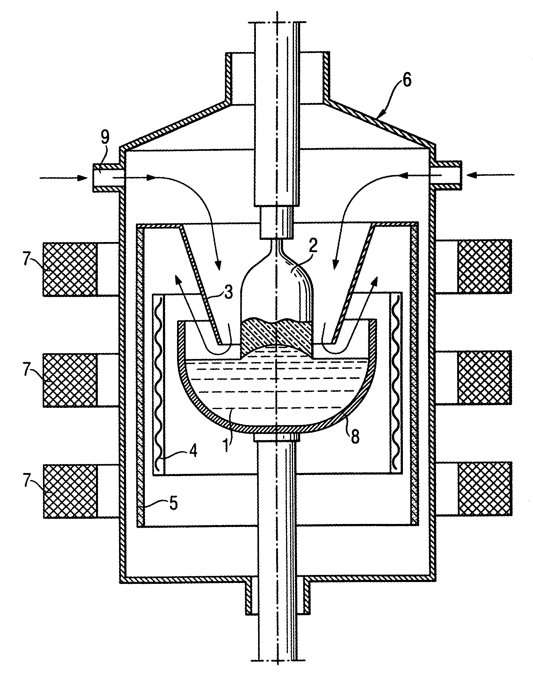
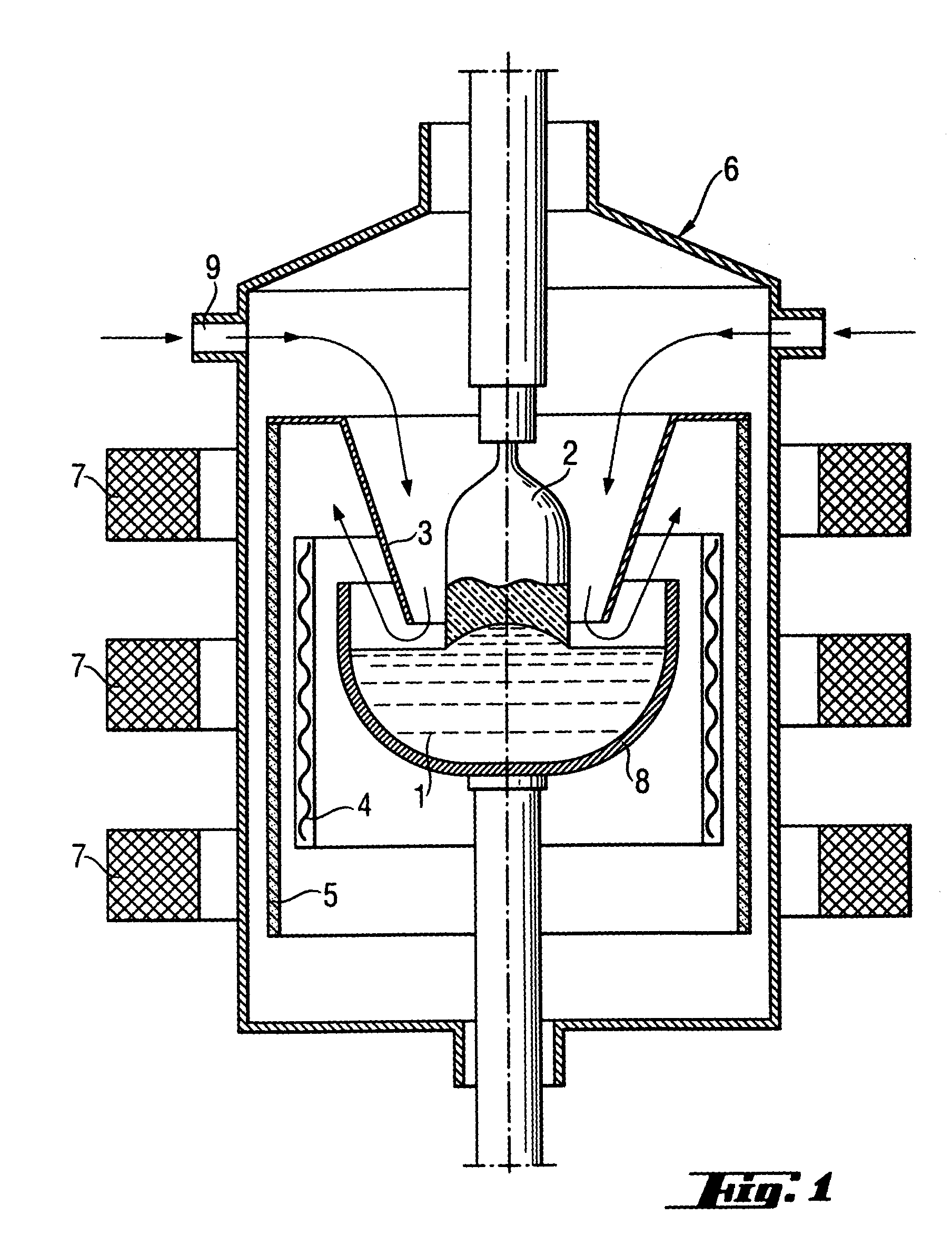
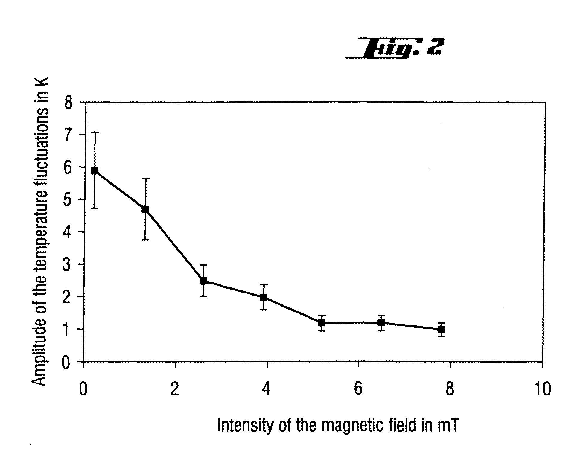
[0023]An apparatus as shown in FIG. 1 having three coils with 36, 40 and 36 turns, connected with phase angles of 0°-120°-240°, was used. The temperature of the melt was measured using submerged thermocouples. The crucible used had a diameter of 14 inches and contained 20 kg of silicon. FIG. 2 shows how low-frequency temperature fluctuations in the melt decrease as the intensity of the magnetic field rises. An intensity of 6 mT corresponds to a current intensity of 81 A.

example 2

[0024]An apparatus as shown in FIG. 1 having three coils each with 20 turns was used. The current intensities were 350 A in each coil, corresponding to 7000 ampere turns. The quartz crucible used had a diameter of 24 inches and contained a sufficient silicon melt to allow a single crystal with a diameter of 300 mm to be pulled. Four silicon single crystals were pulled under virtually identical conditions. Only the frequency and the direction of the traveling movement of the magnetic field differed. FIG. 3 makes it clear that the inclusion of oxygen in the single crystal is considerably higher if the force generated by the magnetic field is directed downward. By contrast, a change in frequency has only a slight effect on the oxygen concentration in the silicon single crystal.

example 3

[0025]A plurality of silicon single crystals with a diameter of 300 mm were pulled under different conditions and at different pulling rates. The pulling rates were selected up to a rate which just still allowed a silicon single crystal of the desired round shape to be pulled. Four fundamentally different pulling conditions were investigated, specifically standard conditions without the application of a magnetic field; conditions under which the melt was under the influence of a static CUSP field; and conditions according to the invention with a traveling magnetic field and a force directed downward (−) or upward (+). For tests which took place under conditions according to the invention, an apparatus as shown in FIG. 1 with a coil system in accordance with Example 2 was used. In all cases, the crucible used had a diameter of 28 inches. FIG. 4 shows that the highest pulling rates can be achieved with the process according to the invention. It is most advantageous if the traveling ma...


PUM

PropertyMeasurementUnit
diameteraaaaaaaaaa
diameteraaaaaaaaaa
diametersaaaaaaaaaa

Abstract

A process for producing a silicon single crystal is by pulling the single crystal from a silicon melt which is contained in a crucible with a diameter of at least 450 mm, above which a heat shield is arranged. The single crystal being pulled has a diameter of at least 200 mm. The silicon melt is exposed to the influence of a traveling magnetic field which exerts a substantially vertically oriented force on the melt in the region of the crucible wall. There is also an apparatus which is suitable for carrying out the process.

Description

BACKGROUND OF THE INVENTION[0001]1. Field of the Invention[0002]The present invention relates to a process for producing a silicon single crystal, by pulling the silicon single crystal from a silicon melt which is contained in a crucible and is exposed to the influence of a traveling magnetic field. The invention also relates to an apparatus which is suitable for carrying out the process.[0003]2. The Prior Art[0004]DE-37 01 733 A1 describes a process of the abovementioned type. The traveling magnetic field is used to reduce the extent to which oxygen is included in the single crystal.SUMMARY OF THE INVENTION[0005]By contrast, the present invention pursues different, in some cases contradictory objectives. It relates to a process for pulling silicon single crystals which have a diameter of at least 200 mm, in particular silicon single crystals belonging to the most modern generation, with diameters of 300 mm and above. The production of crystals of this type requires overcoming a ser...

Claims


Application Information

Patent Timeline
Patent Type & Authority Patents(United States)
IPC IPC(8): C30B15/00C30B29/06C30B15/06C30B15/30
CPCC30B15/305C30B29/06C30B15/06
Inventor VIRBULIS, JANISVON AMMON, WILFRIEDTOMZIG, ERICHGELFGAT, YURIGORBUNOV, LENOID
Owner SILTRONIC AG
Why Eureka
Try Eureka