
Drive circuit and inverter for voltage driving type semiconductor device

Inactive Publication Date: 2010-08-24
HITACHI LTD
View PDF8 Cites 16 Cited by
  • Summary
  • Abstract
  • Description
  • Claims
  • Application Information

AI Technical Summary

Benefits of technology

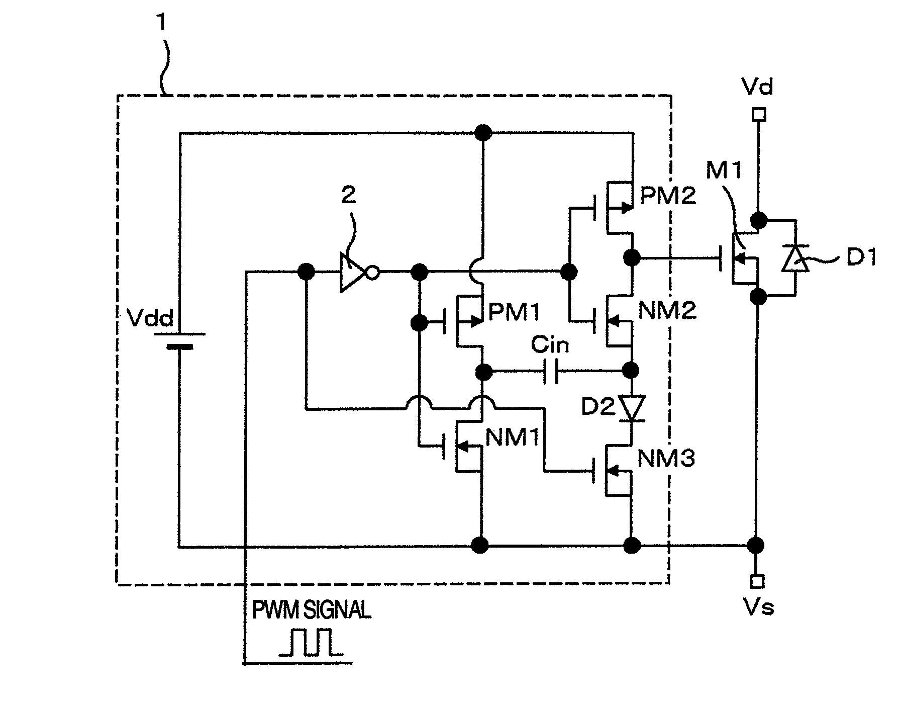
[0012]The present invention has been made to solve the above-described problems of the conventional techniques, and therefore, has an object to provide a drive circuit of a voltage driving type semiconductor element, and an inverter apparatus, which are capable of preventing erroneous ignition without increasing conduction loss thereof, while using only a power supply having a positive voltage.
[0015]As previously described, in accordance with the present invention, the gate of the voltage driving type semiconductor element operated under the OFF state can be maintained at the negative potential only by employing the power supply having the positive voltage. As a result, while the cost, the size, and the conduction loss of the drive circuit are not increased, it is possible to avoid the voltage driving type semiconductor element being erroneously ignited.

Problems solved by technology

As a result, while the cost, the size, and the conduction loss of the drive circuit are not increased, it is possible to avoid the voltage driving type semiconductor element being erroneously ignited.

Method used


Image

  • Drive circuit and inverter for voltage driving type semiconductor device
  • Drive circuit and inverter for voltage driving type semiconductor device
  • Drive circuit and inverter for voltage driving type semiconductor device

Examples


Embodiment Construction

[0032]Referring now to the drawings, a description is made of various embodiments of the present invention.

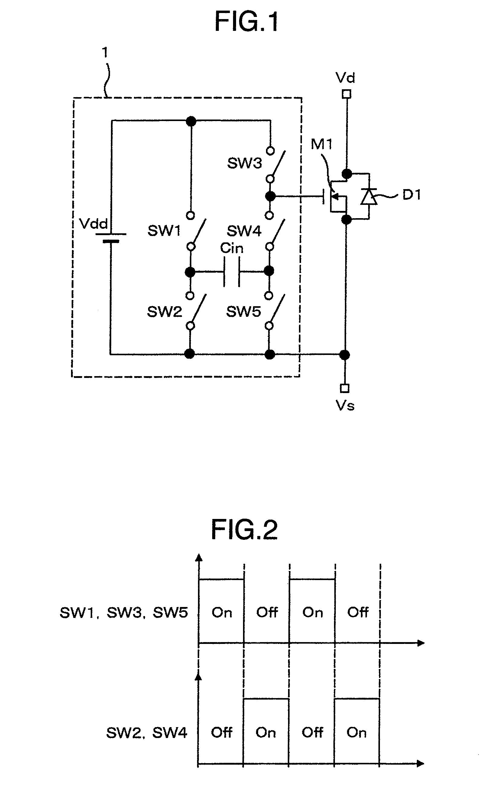
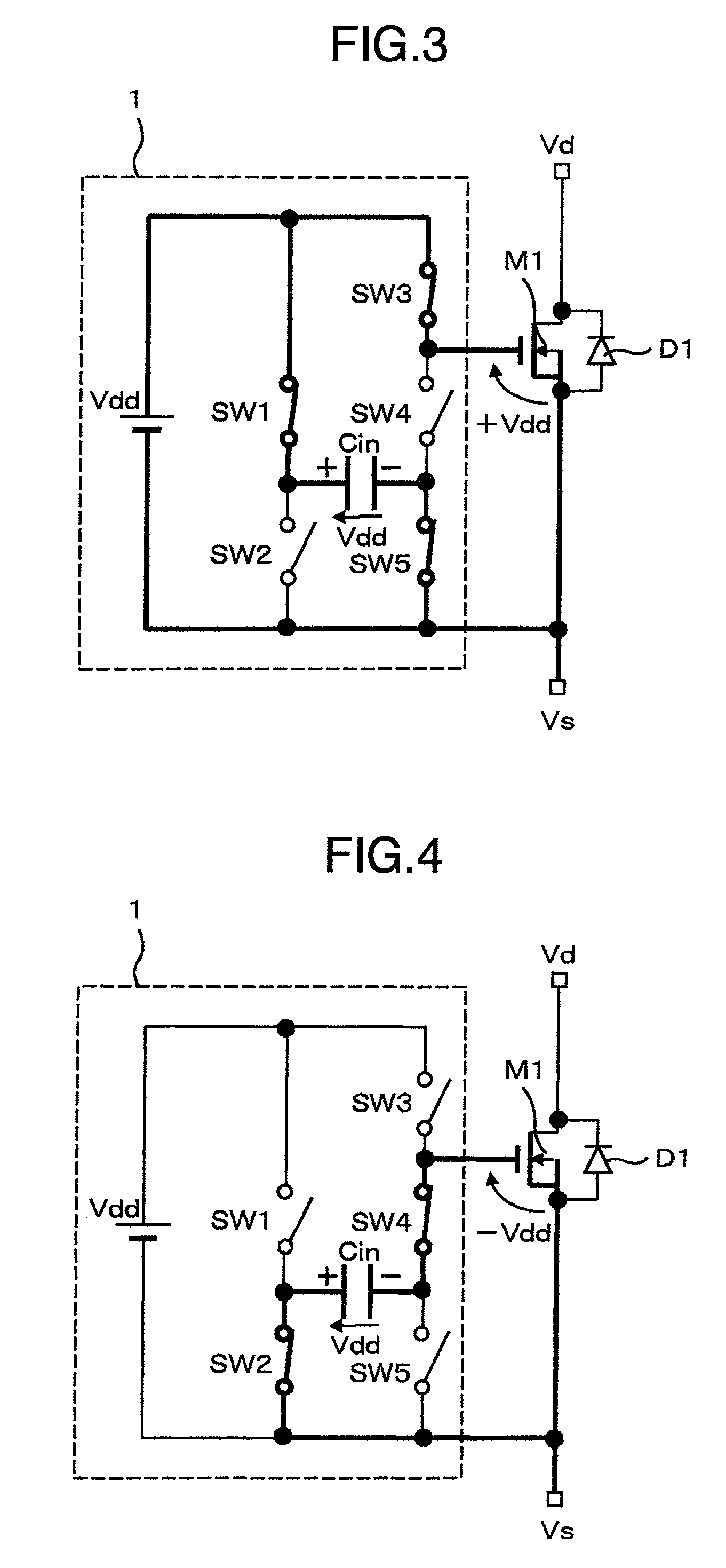
[0033]FIG. 1 is a structural diagram for showing a drive circuit of a voltage driving type semiconductor element according to a first embodiment of the present invention, namely an exemplification in which a power MOSFET “M1” is represented as the above-described voltage driving type semiconductor element. The circuit arrangement of the first embodiment is constituted by a diode “D1” built in the power MOSFET “M1”, a drive circuit 1 of the power MOSFET “M1”, a DC power supply “Vdd”, first to fifth switches “SW1” to “SW5”, and a capacitor “Cin.” The first switch “SW1” is connected to a positive side of the DC power supply “Vdd”; the second switch “SW2” is connected to both the other terminal of the first switch “SW1” and a negative side of the DC power supply “Vdd”; the third switch “SW3” is connected to the positive side of the DC power supply “Vdd”; the fourth switch “SW4” is ...


PUM


Abstract

A drive circuit for driving a semiconductor element is equipped with: a first switch connected to a positive side of a DC power supply; a second switch connected to the other terminal of the first switch and to a negative side of the DC power supply; a third switch connected to the positive side of the DC power supply; a fourth switch connected to the other terminal of the third switch; a fifth switch connected to the other terminal of the fourth switch and to the negative side of the DC power supply; and a capacitor connected to the other terminal of the first switch and to the other terminal of the fourth switch. A gate of the semiconductor element is connected to the other terminal of said third switch; and a source of the semiconductor element is connected to the negative side of the DC power supply.

Description

BACKGROUND OF THE INVENTION[0001]The present invention is related to a drive circuit of a voltage driving type semiconductor element which is employed in a power converter, and also related to an inverter apparatus.[0002]Voltage driving type semiconductor elements such as power MOSFETs (Metal Oxide Semiconductor Field-Effect Transistors) and IGBTs (Insulated-Gate Bipolar Transistors) have a large number of such merits that drive circuits thereof can be made compact and can be operated with low losses, as compared with current driving type semiconductor elements such as thyristors. FIG. 10 is a structural diagram of a single-phase inverter with employment of power MOSFETs as the above-described voltage driving type semiconductor elements.[0003]In the structural diagram of FIG. 10, the single-phase inverter has been equipped with power MOSFETs “M1” to “M4”, diodes “D1” to “D4” which have been built in these power MOSFETs “M1” to “M4”, a power supply voltage “Vin”, and an inductor 14 w...

Claims


Application Information

Patent Timeline
IPC IPC(8): H03K3/00
CPCH02M3/07H02M1/08H02M2003/071H02M7/5387H02M3/071H03K17/00
Inventor HASHIMOTO, TAKAYUKIHIRAO, TAKASHISHIRAISHI, MASAKI
Owner HITACHI LTD
Learn More