Semiconductor device

a technology of semiconductors and devices, applied in the direction of pulse generators, pulse techniques, machines/engines, etc., can solve the problems of ignition plug discharge, unintended timing and damage to the engine, ignition plug erroneous ignition, etc., and achieve the effect of avoiding erroneous ignition of the ignition plug

Active Publication Date: 2015-01-06
FUJI ELECTRIC CO LTD
View PDF6 Cites 6 Cited by
  • Summary
  • Abstract
  • Description
  • Claims
  • Application Information

AI Technical Summary

Benefits of technology

[0031]Embodiments of the invention are directed to these and other shortcomings. Certain embodiments provide a semiconductor device with a small size avoiding erroneous ignition of the ignition plug by suppressing oscillation of collector current Ic of the output stage IGBT in operation of the current control circuit and in operation of the self shut down circuit.
[0040]In some embodiments, a semiconductor device includes a pulse generating circuit, a switching circuit, and a current source circuit and performing a current control function and a self shut down function in which pulse current is generated with the pulse generating circuit, the switching circuit and the current source circuit, and the charges on a capacitor is discharged by the pulse current in the process of self shut down. Thus, the collector current Ic of the output stage IGBT does not oscillate in operation of the current control circuit and in operation of the self shut down circuit, thereby avoiding erroneous ignition of the ignition plug. In some embodiments, the pulsed discharge can allow for a relatively small sized capacitor thereby providing a small sized semiconductor device.

Problems solved by technology

However, abrupt shut down of the Ic may cause discharges of the ignition plug 505 at an unintended timing and damage to the engine.
This abrupt falling down of the gate voltage VGout generates oscillation in the current Ic and may cause erroneous ignition of the ignition plug 505.
The conventional semiconductor device for ignition shown in FIG. 12 may generate oscillation in the collector current Ic of the output stage IGBT in an operation time of the current control circuit or in an operation time of the self shut down circuit and cause erroneous ignition of the ignition plug.
However, the documents do not mention a countermeasure against oscillation of collector current Ic of the output stage IGBT in operation of the self shut down circuit, and thus have the similar problem to the one in the conventional semiconductor device for ignition shown in FIG. 12.

Method used


Image

  • Semiconductor device
  • Semiconductor device
  • Semiconductor device

Examples


first embodiment

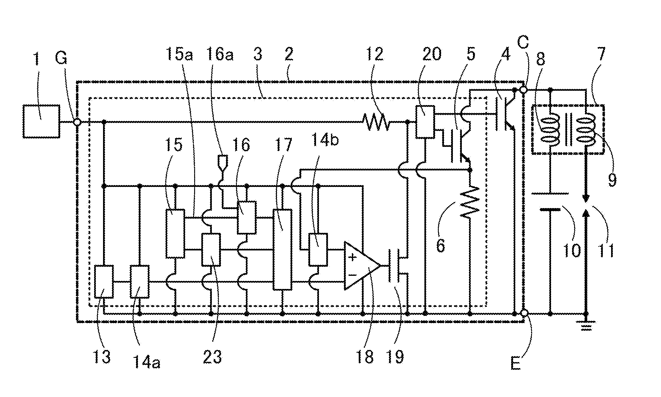
[0056]FIG. 1 shows a construction of a portion of a semiconductor device according to a first embodiment of the present invention. This semiconductor device is a semiconductor device for ignition performing a current control function and a self shut down function, although the invention can also be directed to other uses. In the following description, MOSFET is abbreviated to “MOS.”

[0057]This semiconductor device comprises an ECU 1, an ignition IC 2, an ignition coil 7, a voltage source 10, and an ignition plug 11.

[0058]The ignition IC 2 includes an output stage IGBT 4 for ON / OFF control of the primary current through the ignition coil 7 and a current control circuit 3 for control the primary current of the ignition coil 7. The ignition IC 2 has three terminals of a collector terminal or a C-terminal connecting to the ignition coil 7, an emitter terminal or an E-terminal connecting to GND, and a gate terminal or a G terminal connecting to the ECU 1.

[0059]The current control circuit ...

second embodiment

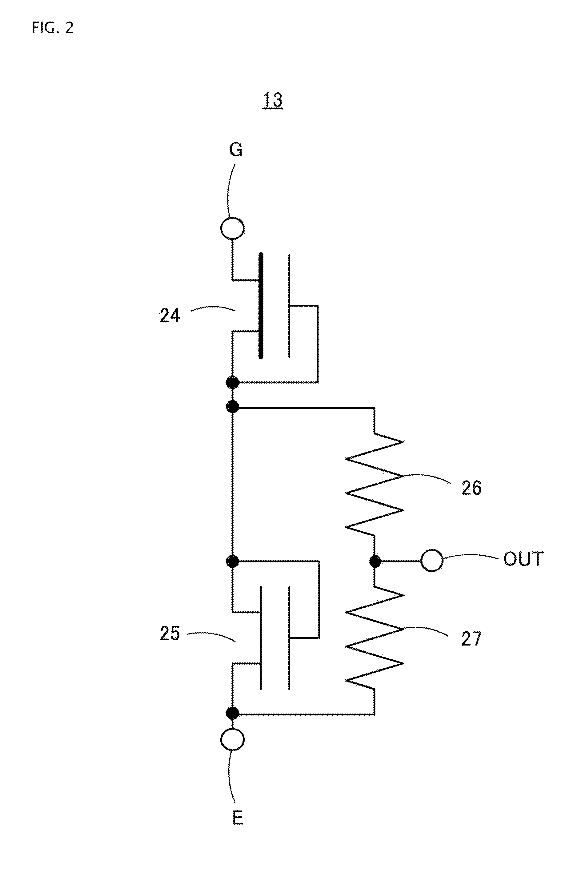
[0079]FIG. 11 shows an example of construction of a semiconductor device according to a second embodiment of the present invention. The figure illustrates solely the circuit construction of the self shut down circuit 17 composing the semiconductor device. Circuit construction other than the self shut down circuit 17 in the Second Embodiment is generally the same as the one in the First Embodiment.

[0080]In the self shut down circuit 17 of FIG. 11, one end of the switching circuit 22 is connected to the gate terminal of the MOS 43 and the other end is connected to the E terminal. The pulse signal inverted in the inverter 46 controls ON / OFF of the switching circuit 22. In the ON state of the switching circuit 22, the gate terminal of the MOS 43 is pulled down to interrupt the output current of the current source circuit 21. Discharging operation of the charges on the capacitor 44 in a pulsed mode in the process of self shut down is conducted in the same manner as the operation in the s...


PUM


Abstract

A semiconductor device for ignition performing a current control function and a self shut down function can include a pulse generating circuit, a switching circuit, and a current source circuit, the three circuits together generating a pulse current that discharges a capacitor in the self shut down process. This construction can serve to suppress oscillation of a collector current Ic of the output stage IGBT in the operating processes of the current control circuit and the self shut down circuit, thus preventing or minimizing the likelihood of the ignition plug from erroneous ignition. In addition, the discharge of the capacitor in a pulsed mode can allow for down-sizing of the capacitor, which can contribute to minimization of the semiconductor device.

Description

BACKGROUND OF THE INVENTION[0001]1. Field of the Invention[0002]Embodiments of the invention relate to semiconductor devices for use in ignition devices for, for example, internal combustion engines.[0003]2. Description of the Related Art[0004]An ignition device for an internal combustion engine of a vehicle uses a semiconductor device installing a power semiconductor element for switching control of a primary current in an ignition coil. FIG. 12 shows an example of construction of a conventional, general semiconductor device for ignition of an internal combustion engine using a power semiconductor element of an insulated gate bipolar transistor (IGBT).[0005]The semiconductor device for ignition shown in FIG. 12 includes an engine control unit (ECU) 501, which is an electronic control unit, a semiconductor integrated circuit (IC) for ignition (an ignition IC) 502, an ignition coil 503, a voltage source 504, and an ignition plug 505.[0006]The ignition IC 502 includes an output stage ...

Claims


Application Information

Patent Timeline
Patent Type & Authority Patents(United States)
IPC IPC(8): H03L7/00F02P3/055F02P9/00H03K3/57
CPCH03K3/57F02P3/0554F02P9/005
Inventor MIYAZAWA, SHIGEMI
Owner FUJI ELECTRIC CO LTD
Why Eureka
Try Eureka