Interference analysis method, interference analysis device, interference analysis program and recording medium with interference analysis program recorded thereon

a technology of interference analysis and interference analysis, which is applied in the direction of instruments, analogue processes for specific applications, electric/magnetic computing, etc., can solve the problems of interference between wirings, serious problems, and demands for electronic circuits to realize speedy operation and miniaturization, and achieve the effects of reducing load, short time period, and high speed

Inactive Publication Date: 2010-08-31
PANASONIC CORP
View PDF14 Cites 0 Cited by
  • Summary
  • Abstract
  • Description
  • Claims
  • Application Information

AI Technical Summary

Benefits of technology

[0043]Therefore, with the foregoing in mind, it is an object of the present invention to provide an interference analysis method, an interference analysis device, an interference analysis program and a recording medium with an interference analysis program recorded thereon, by which the interference between wirings can be analyzed at high speed, with a reduced load and in a short time period.
[0048]According to the interference analysis method, the interference analysis device, the interference analysis program and the recording medium with an interference analysis program recorded thereon of the present invention, the interference between wirings can be analyzed at high speed, with a reduced load and for a short time period.

Problems solved by technology

When designing a high-frequency circuit with the procedure shown in FIG. 9, a serious problem occurs, called interferences due to electromagnetic induction between wirings.
This is a problem of the interference between wirings.
Meanwhile, there are demands for electronic circuits realizing a speedy operation and miniaturization.
In such an electronic circuit with a high frequency current flowing through the wirings thereon and with a short distance between the wirings, the influence of the interference between wirings is considerable, thus posing a serious challenge.
Further, in addition to between the wirings of the board 950 and between the components mounted thereon, the same problem may occur, for example, between wirings in one LSI chip and between cells connected with such wirings.
A wiring pattern 1000 shown in FIG. 11A is so complicated that the electromagnetic field analysis cannot be performed for such a state of the wiring pattern.

Method used


Image

  • Interference analysis method, interference analysis device, interference analysis program and recording medium with interference analysis program recorded thereon
  • Interference analysis method, interference analysis device, interference analysis program and recording medium with interference analysis program recorded thereon
  • Interference analysis method, interference analysis device, interference analysis program and recording medium with interference analysis program recorded thereon

Examples


embodiment 1

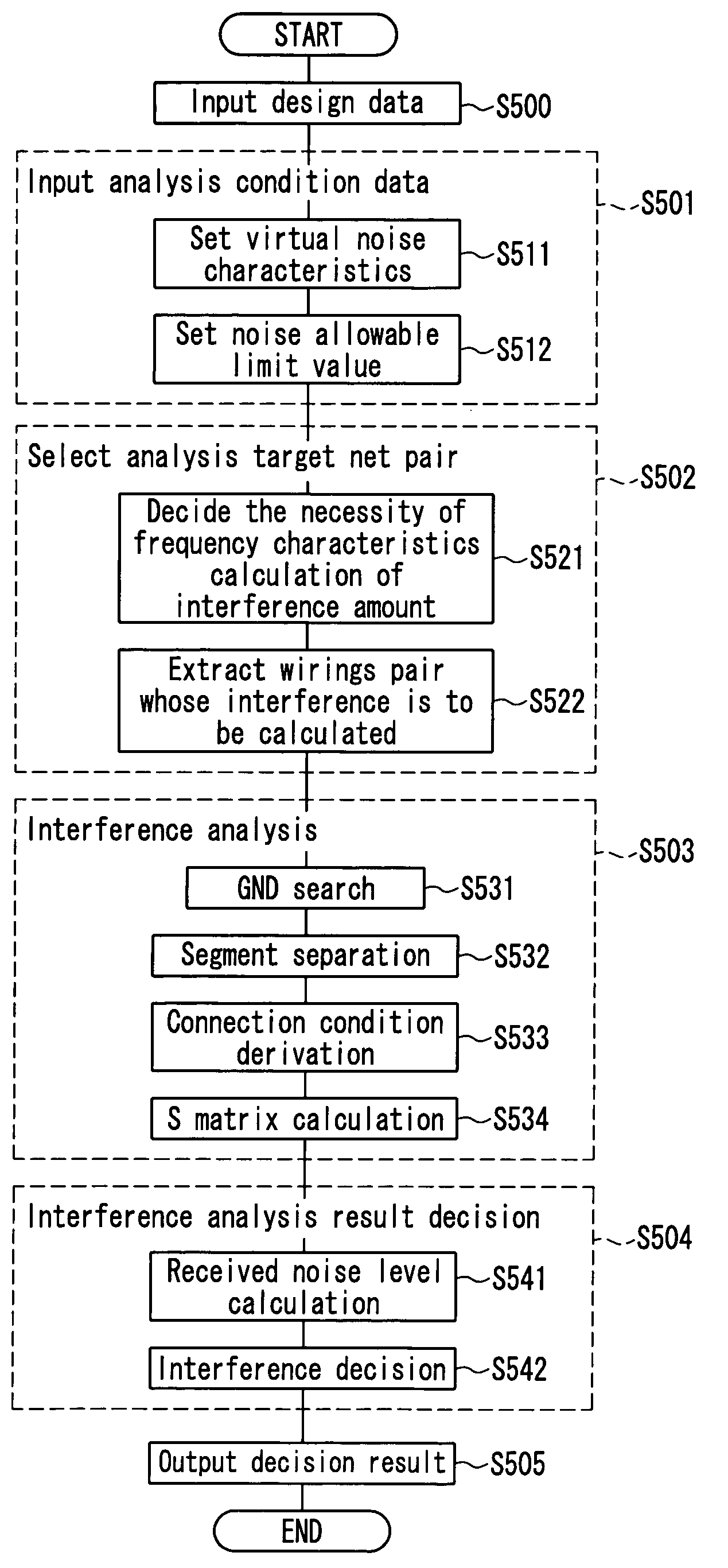
[0087]Embodiment 1 relates to an interference analysis method and an interference analysis device for alleviating a designing load of a high frequency circuit, and also relates to a program that makes a computer execute the procedure for embodying the interference analysis method and the interference analysis device and a recording medium with this program recorded thereon.

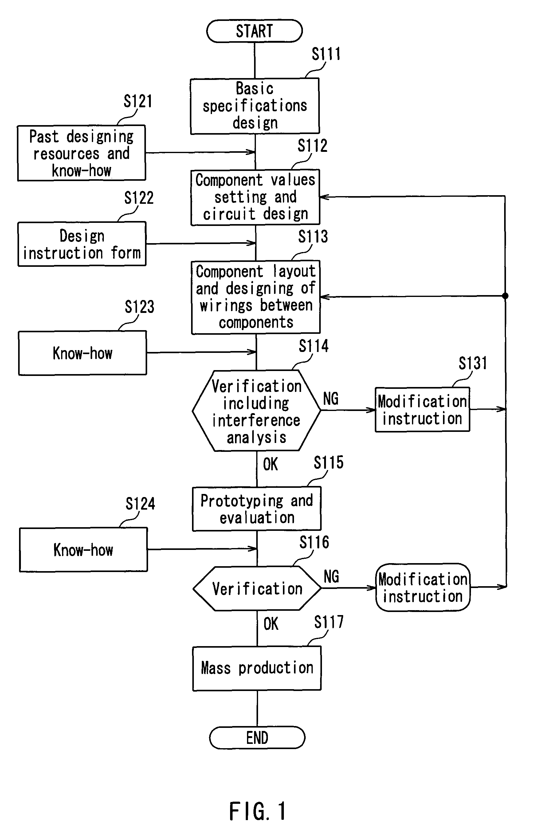
[0088]FIG. 1 is a flowchart showing the outline procedure of high-frequency circuit design, which is performed using the interference analysis method according to the present embodiment.

[0089]The outline procedure shown in FIG. 1 is similar to the outline procedure of the conventional digital circuit design shown in FIG. 9 in many respects, and therefore such similar respects will be described briefly and different points will be described in detail.

[0090]According to this design process, firstly, basic specifications are designed (S111). The design of the basic specifications does not involve the specific configu...


PUM


Abstract

An interference analysis device can be provided, which analyzes interference between wirings of a circuit board with reduced load and for a short time period. The interference analysis device according to the present invention includes: a design data input part for inputting design data of the circuit board; a noise characteristics setting part that sets data representing electrical characteristics of noise for a wiring of the circuit board; a limit value setting part that sets an allowable limit value of noise received by a wiring; a selection part that selects a wiring group to be analyzed based on the noise characteristics data and the allowable limit value; an interference analysis part that calculates, concerning the selected wiring group, an amount of interference from a wiring giving the interference to a wiring receiving the interference; and a received noise level calculation part that calculates a noise level that the wiring receiving the interference will receive.

Description

BACKGROUND OF THE INVENTION[0001]1. Field of the Invention[0002]The present invention relates to a method and a device for analyzing mutual interference due to electromagnetic induction between wirings formed in a circuit board by a computer and investigating an influence thereof. The present invention also relates to a program making a computer execute such an analysis procedure and a recording medium with the program recorded thereon.[0003]2. Related Background Art[0004]Conventionally, as methods and devices for analyzing mutual interference due to electromagnetic induction between wirings formed in a circuit board and investigating an influence thereof, a noise checking method and such a device described in JP2000-035984A, for example, are available.[0005]FIG. 9 is a flowchart showing the outline procedure of conventional digital circuit design.[0006]According to this design process, firstly, basic specifications are designed (S911). The design of the basic specifications does no...

Claims


Application Information

Patent Timeline
Patent Type & Authority Patents(United States)
IPC IPC(8): G06F17/50G01R31/28H01L21/82
CPCG06F17/5036G06F30/367
Inventor IWAKI, HIDEKIOGURA, TETSUYOSHIKOMATSU, NAOKINAKAYAMA, TAKESHIKINOSHITA, TOMOHIRO
Owner PANASONIC CORP
Why Eureka
Try Eureka