High-performance FET device layout

a transistor and high-performance technology, applied in the field of field-effect transistors, can solve the problems of inability to sustain the trend of decreasing technology groundrules to increase performance, adversely affect the scalability of integrated circuit performance,

Inactive Publication Date: 2010-09-07
GLOBALFOUNDRIES INC
View PDF9 Cites 11 Cited by
  • Summary
  • Abstract
  • Description
  • Claims
  • Application Information

AI Technical Summary

Benefits of technology

[0004]A first aspect of the present invention is a method, comprising: selecting a reference design for a field effect transistor, the field effect transistor including a source, a drain, a channel between the source and drain, a gate electrode over the channel, one or more source contacts to the source and one or more drain contacts to the drain, each of the one or more source contacts spaced a first distance from the gate electrode and each of the one or more drain contacts spaced a second distance from the gate electrode; and adjusting the first distance and the second distance to maximize a performance parameter of the field effect transistor to create a fast design for the field effect transistor.
[0010]A seventh aspect of the present invention is the first aspect, further including: limiting an amount of the adjusting the first and second distances to prevent a total area of the field effect transistor from exceeding a pre-determined limit.

Problems solved by technology

A most important issue for the semiconductor industry is integrated circuit performance scalability.
In general, scalability is adversely affected by the non-scalability of complementary metal-oxide-silicon (CMOS) device technology groundrules below about 250 nm and the non-scalability of process tolerances.
Without some technique to overcome CMOS scalability, the trend of decreasing technology groundrules to increase performance cannot be sustained.

Method used


Image

  • High-performance FET device layout
  • High-performance FET device layout
  • High-performance FET device layout

Examples


Embodiment Construction

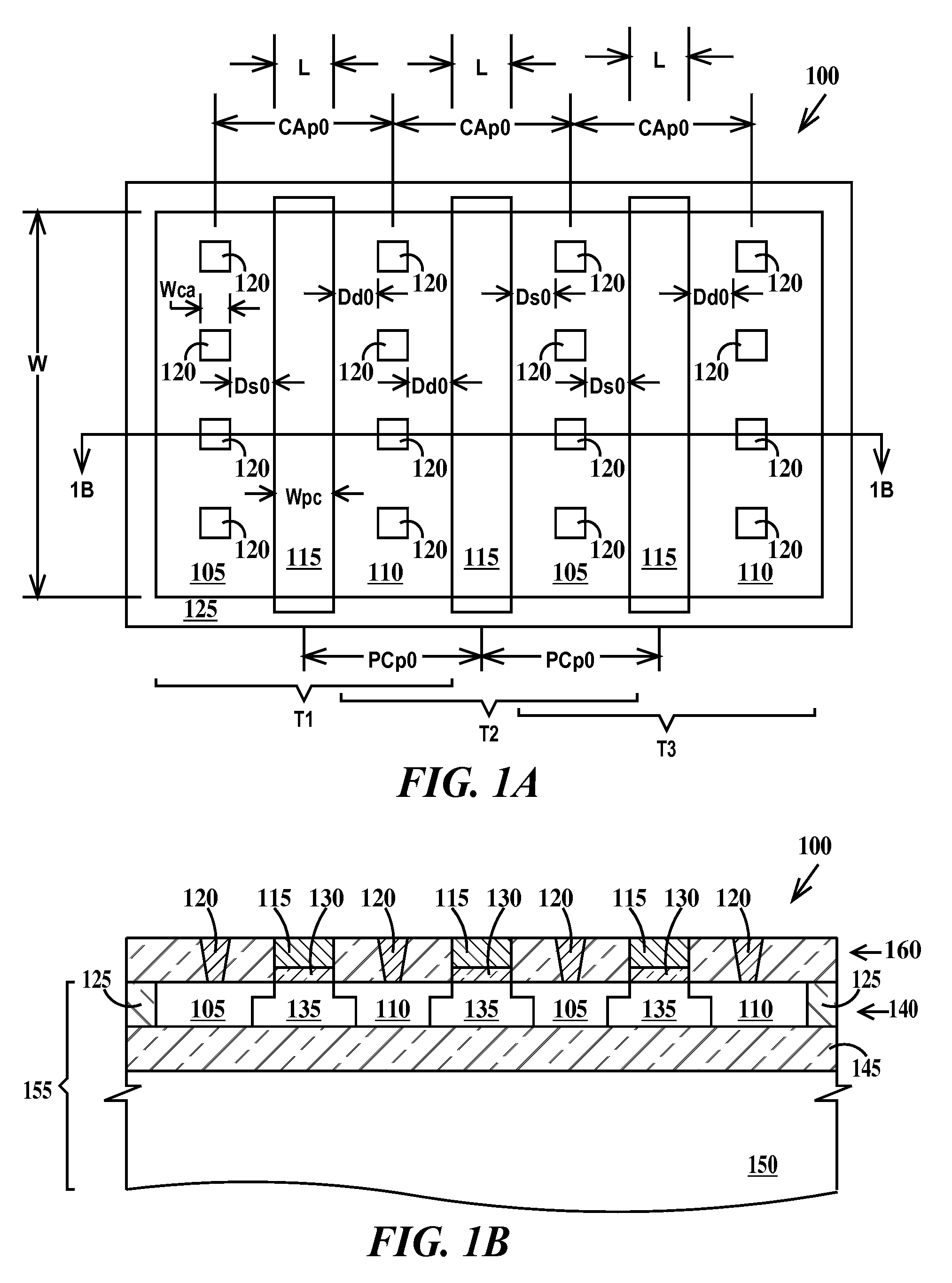
[0032]FIG. 1A is a top view and FIG. 1B is a cross-sectional view through line 1B-1B of FIG. 1A of an exemplary reference FET layout not optimized for performance according to embodiments of the present invention. In FIG. 1A, a device 100 includes sources 105 and drains 110 and gate electrodes 115 on opposite sides of the source / drains. Device 100 comprises three reference transistors T1, T2 and T3 with transistors T1 and T2 sharing a common drain and transistors T2 and T3 sharing a common source. Transistor T1, T2 and T3 may be N-channel field effect transistors (FETs) or NFETs or P-channel FETs or PFETs. Each of transistors T1, T2 and T3 have a channel width W in a widthwise direction and a channel length L in a lengthwise direction, the widthwise and lengthwise directions being perpendicular. The extent of L depends upon how far sources 105 and drains 110 extend under gate electrodes 115.

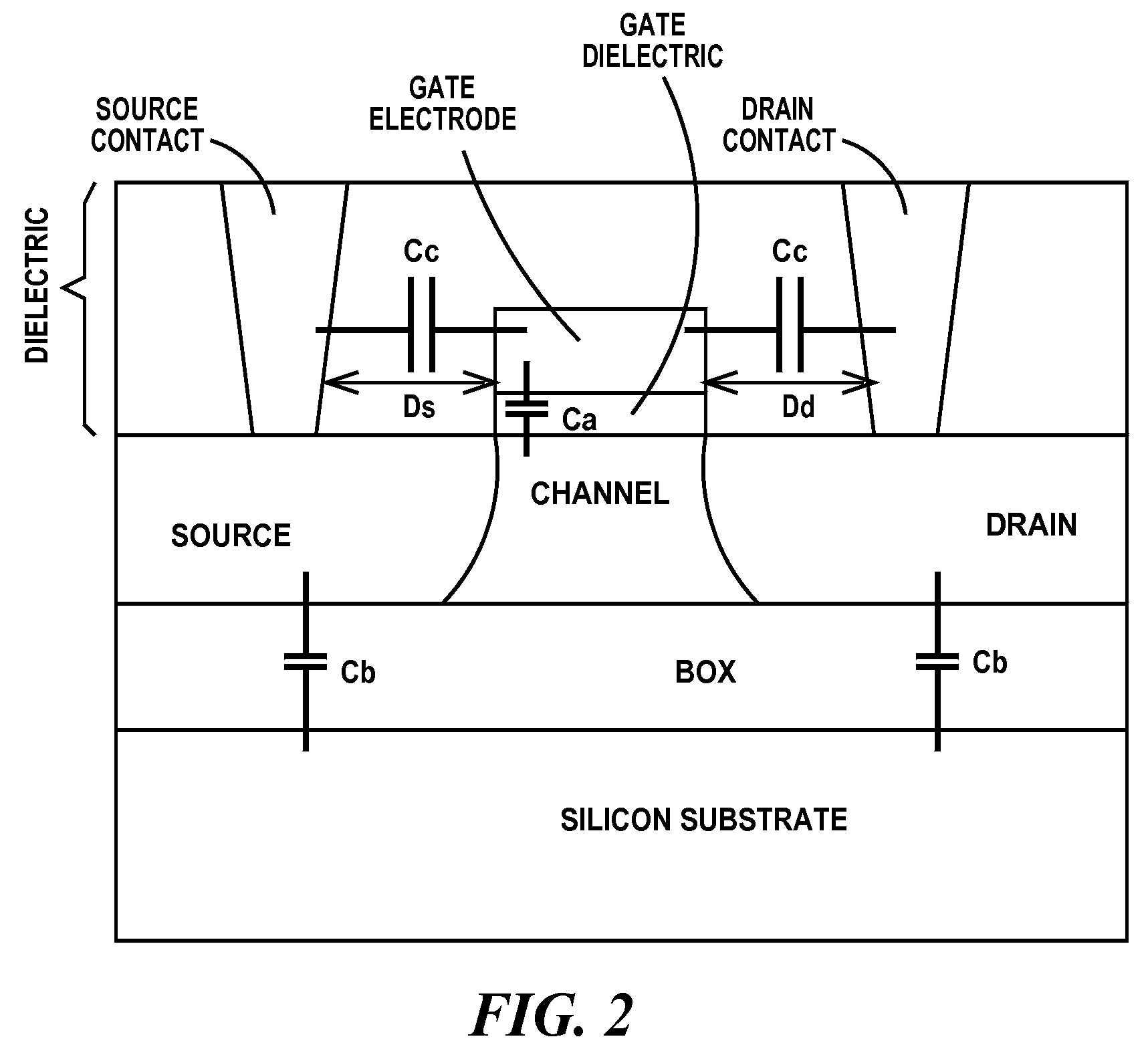
[0033]A set of source / drain contacts 120 are formed over sources 105 and drains 110. Device 1...


PUM


Abstract

A fast FET, a method and system for designing the fast FET and a design structure of the fast FET. The method includes: selecting a reference design for a field effect transistor, the field effect transistor including a source, a drain, a channel between the source and drain, a gate electrode over the channel, at least one source contact to the source and at least one contact to the drain, the at least one source contact spaced a first distance from the gate electrode and the at least one drain contact spaced a second distance from the gate electrode; and adjusting the first distance and the second distance to maximize a performance parameter of the field effect transistor to create a fast design for the field effect transistor.

Description

[0001]This Application is related to U.S. patent application Ser. No. 11 / 550,818, filed Oct. 19, 2006.FIELD OF THE INVENTION[0002]The present invention relates to the field of field effect transistors (FET); more specifically, it relates to an FET having a gate to source / drain spacing optimized for improved FET performance, a method and system for determining the gate to source / drain spacing for optimizing the performance of the FET, and a design structure for an FET having a gate to source / drain spacing optimized for improved FET performance.BACKGROUND OF THE INVENTION[0003]A most important issue for the semiconductor industry is integrated circuit performance scalability. Scalability is the tracking of performance with decreased transistor size. In general, scalability is adversely affected by the non-scalability of complementary metal-oxide-silicon (CMOS) device technology groundrules below about 250 nm and the non-scalability of process tolerances. Without some technique to over...

Claims


Application Information

Patent Timeline
Patent Type & Authority Patents(United States)
IPC IPC(8): H01L29/786
CPCH01L27/0207H01L29/4238H01L21/84
Inventor KIM, JONGHAELEE, SUNGJAEPLOUCHART, JEAN-OLIVIERSPRINGER, SCOTT KEITH
Owner GLOBALFOUNDRIES INC
Why Eureka
Try Eureka