Electrooptic device and electronic device including the same

a technology of electronic devices and optical components, applied in the field of optical components, can solve the problems of reducing the display quality, reducing the image quality, and the shielding layer on the dustproof substrate may not provide sufficient light shielding effect in the vicinity of the frame, so as to achieve the effect of improving the light shielding

Active Publication Date: 2010-10-05
138 EAST LCD ADVANCEMENTS LTD
View PDF13 Cites 36 Cited by
  • Summary
  • Abstract
  • Description
  • Claims
  • Application Information

AI Technical Summary

Benefits of technology

[0007]An advantage of some aspects of the invention is to provide an electrooptic device having improved light shielding effect in the vicinity of the frame of the display region and an electronic device including the same.

Problems solved by technology

In the case where the liquid crystal device is used for a light valve of a liquid crystal projector, when dust particles (hereinafter, simply referred to as dust) adhere to the surface of the light valve, the image of the dust is also projected to a screen to raise the possibility of projecting the dust image on the screen, thus decreasing the quality of the image.
This may cause leakage of light from the clearance between the frame light shielding layer and the sealing region to decrease the display quality.
However, when the frame light shielding layer on the opposing substrate and the light shielding layer on the dustproof substrate become out of agreement, the light shielding layer on the dustproof substrate may not provide sufficient light shielding effect in the vicinity of the frame.

Method used


Image

  • Electrooptic device and electronic device including the same
  • Electrooptic device and electronic device including the same
  • Electrooptic device and electronic device including the same

Examples


Embodiment Construction

[0039]Embodiments of the invention will be described with reference to the drawings. The following embodiment(s) takes a TFT active matrix drive system liquid crystal device as an example of the electrooptic device of the invention.

[0040]A liquid crystal device according to an embodiment will be described with reference to FIGS. 1 to 7.

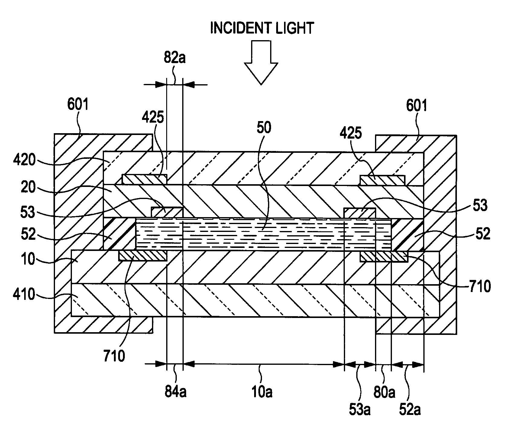
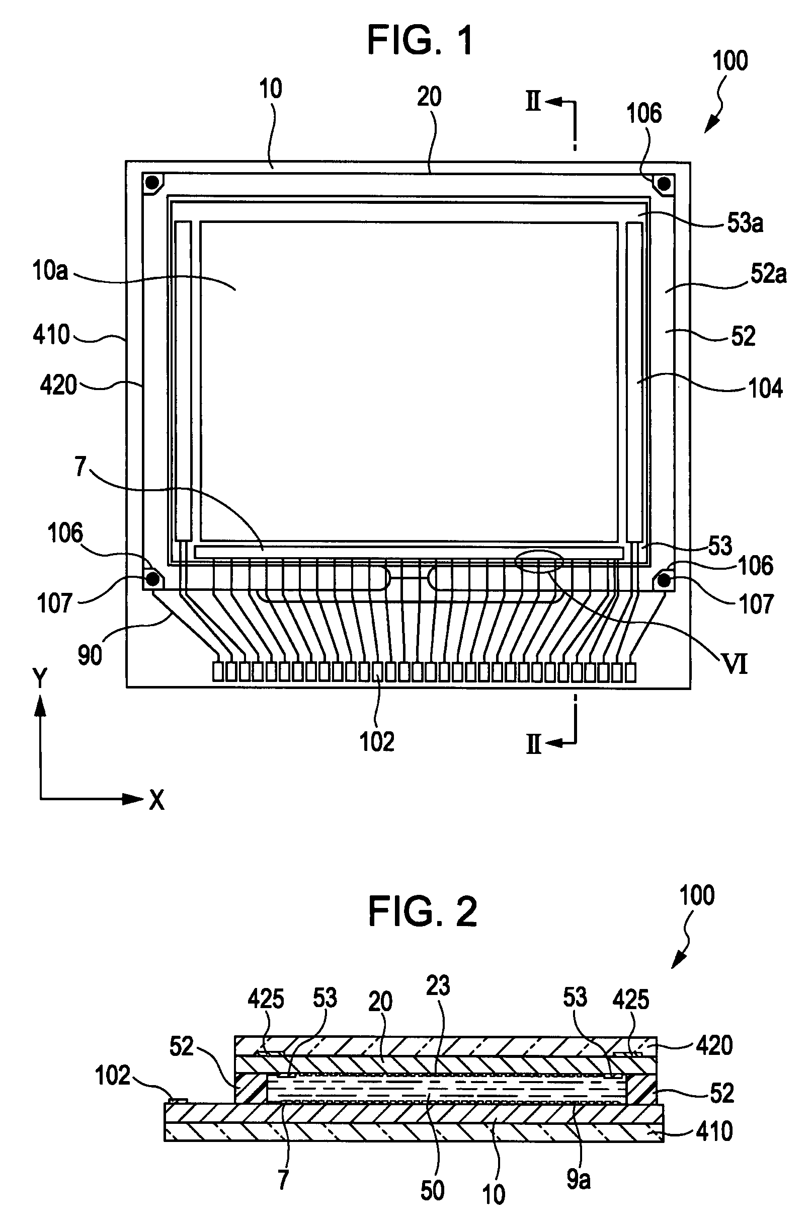
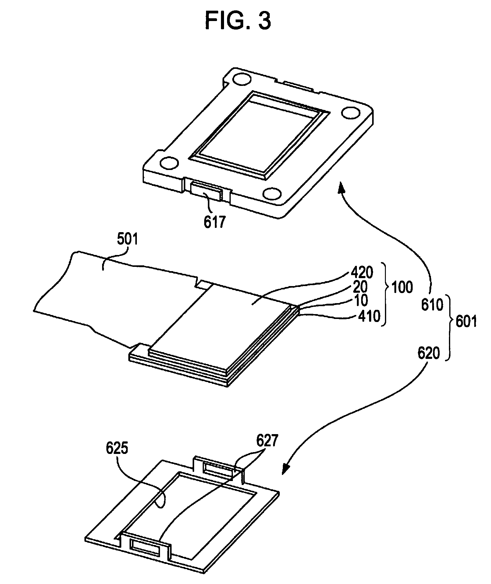
[0041]The overall structure of the liquid crystal device according to the embodiment will be described with reference to FIGS. 1 to 3. FIG. 1 is a plan view of the overall structure of the liquid crystal device of the embodiment, denoted by reference numeral 100; FIG. 2 is a cross-sectional view taken along line II-II of FIG. 1; and FIG. 3 is an exploded perspective view of a packaging case and the liquid crystal device.

[0042]Referring to FIGS. 1 and 2, the liquid crystal device 100 of the embodiment includes a device substrate 10 and an opposing substrate 20 opposed to each other. The device substrate 10 is an example of “a first substrate” of the in...


PUM

PropertyMeasurementUnit
optical densityaaaaaaaaaa
widthaaaaaaaaaa
widthaaaaaaaaaa

Abstract

An electrooptic device includes: a pair of first and second substrates that sandwich an electrooptic material; a plurality of pixel electrodes disposed in a pixel region on the first substrate; a first light shielding layer disposed on the second substrate, the first light shielding layer defining the periphery of the pixel region; a sealing material that bonds the first substrate and the second substrate together in a sealing region around the periphery of a first light shielding region having the first light shielding layer; a dustproof substrate disposed on the surface of the second substrate opposite to the electrooptic material; a second light shielding layer disposed on the dustproof substrate so as to enclose the pixel region; and a third light shielding layer disposed on the dustproof substrate so as to at least partly overlap with the first and second light shielding layers.

Description

BACKGROUND[0001]1. Technical Field[0002]The present invention relates to a technical field of an electrooptic device such as a liquid crystal device and an electric device including the electrooptic device, such as a liquid crystal projector.[0003]2. Related Art[0004]A Liquid crystal device which is an example of this type of electrooptic device is generally constructed such that a device substrate on which pixel electrodes and switching elements are disposed and an opposing substrate on which an opposing electrode is provided are bonded together at a sealing region with a sealing material such as ultraviolet cure resin, with a specified clearance in between, and liquid crystal is sealed between the substrates. In the case where the liquid crystal device is used for a light valve of a liquid crystal projector, when dust particles (hereinafter, simply referred to as dust) adhere to the surface of the light valve, the image of the dust is also projected to a screen to raise the possib...

Claims


Application Information

Patent Timeline
Patent Type & Authority Patents(United States)
IPC IPC(8): G02F1/1333G02F1/1335G03B21/00
CPCG02F1/133512G03B21/14G02F1/136286G02F2001/133311G02F2001/13629G02F1/133311G02F1/13629G02F1/1335
Inventor MOCHIZUKI, HIROAKI
Owner 138 EAST LCD ADVANCEMENTS LTD
Why Eureka
Try Eureka