Ultraviolet light emitting AlGaN composition, and ultraviolet light emitting device containing same

a technology of ultraviolet light and composition, which is applied in the direction of solid-state devices, lasers, semiconductor lasers, etc., can solve the problems of lack of a native substrate for the homoepitaxial growth of epilayers, limited layer quality, and inconvenient use of ingan alloys in uv led's at wavelengths shorter than 365 nanometers, and achieve enhanced radiative efficiency

Inactive Publication Date: 2010-10-12
US SEC THE ARMY THE
View PDF4 Cites 26 Cited by
  • Summary
  • Abstract
  • Description
  • Claims
  • Application Information

AI Technical Summary

Benefits of technology

[0029]In order to achieve the objects of the present invention, as discussed above, the present inventors earnestly endeavored to overcome the difficulties in manufacturing a UV LED composition comprising AlGaN as the active region layer, a method of producing such a composition, and a device containing same. Accordingly, the present inventors have developed a UV LED AlGaN composition active region layer having localized inhomogeneities resulting in carrier localization and enhanced radiative efficiency, and a suitable manufacturing method therefor. As such, in a first embodiment of the present invention, a semiconductor-based ultraviolet light emitting device composition is provided, comprising:

Problems solved by technology

With the proper growth conditions, however, it was discovered that material could be grown in which the indium did not incorporate uniformly throughout the InGaN layer (i.e., the material has areas of high and low concentrations of indium spread throughout).
Unfortunately, InGaN alloys are not suitable for use in UV LED's at wavelengths shorter than 365 nanometers (nm).
A major problem in manufacturing practical III-Nitride based sources, such as AlGaN alloys, is the lack of a native substrate for the homoepitaxial growth of epilayers.
Consequently, most devices are deposited heteroepitaxially on lattice mismatched substrates, like sapphire or SiC, with the resulting layer quality limited by the high density of threading dislocations produced therein.
Such threading dislocations present in AlGaN alloys deposited heteroepitaxially on lattice mismatched substrates are associated with non-radiative recombination centers that compete with radiative recombination paths, thus reducing the radiative recombination efficiency of these materials.
With regard to optical sources, these threading dislocations present in AlGaN alloys deposited heteroepitaxially on lattice mismatched substrates greatly reduce the wall plug efficiency (i.e., the ratio of the power of the light emitted versus the electrical power applied).
The low wall plug efficiency further results in excessive heating of the UV LED material, which reduces the lifetime thereof, and may change the spectral and power output properties of UV LEDs.
Extracting the heat from these devices can also be challenging since the most commonly used substrate, sapphire, is a poor thermal conductor at room temperature.
This difficulty in heat extraction requires elaborate packaging of the UV LED material, such as including flip-chip bonding of the final device to a thermally conductive substrate to help conductively dissipate the heat.
Without the availability of lattice matched substrates with reduced defect density, or the advantages of compositional fluctuations (i.e., localized inhomogeneities) found in InGaN alloys made using the conventional methods of production, production of efficient UV LED using band edge AlGaN alloys has been found to be practically impossible.
These processes, as well as the subsequent buffer layers deposited, greatly affect the number of defects in the material.
While this conventional UV LED device structure is simple to grow, it is not possible to produce efficient DH-UV LEDs using the above-described method, due to the susceptibility of the active region layer to the non-radiative recombination centers typically found in these materials, polarization fields that tend to separate the electron hole pairs, and the lack of quantum confinement to improve electron-hole wave function overlap.
The latter two reasons lead to a longer radiative lifetime in the bulk active layers that does not compete favorably with the non-radiative processes.
This is due to the highly reactive nature of the active nitrogen species generated by the plasma source that results in very short adatom diffusion lengths.
Heavily Ga-rich growth conditions results in the accumulation of liquid Ga metal droplets on the surface of the film.

Method used


Image

  • Ultraviolet light emitting AlGaN composition, and ultraviolet light emitting device containing same
  • Ultraviolet light emitting AlGaN composition, and ultraviolet light emitting device containing same
  • Ultraviolet light emitting AlGaN composition, and ultraviolet light emitting device containing same

Examples


example 1

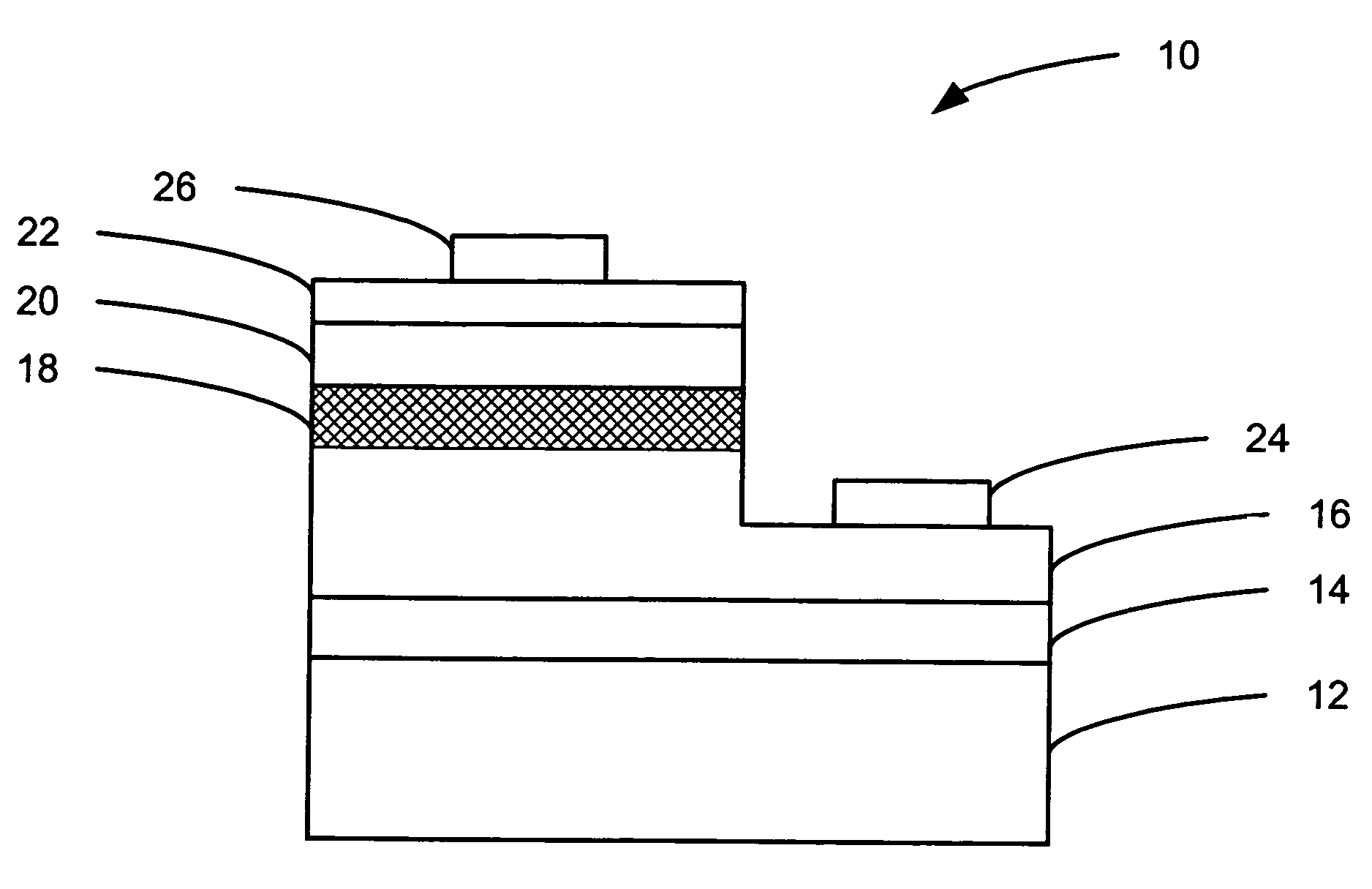
[0141]A DH (double heterostructure) UV-LED was fabricated according to the present method, using PA-MBE as described above. In particular, a n-type AlGaN current spreading layer having an AlN mole fraction of about 40% and a thickness of approximately 50 nm was deposited upon an AlGaN template. This n-type AlGaN current spreading layer was deposited under nitrogen limited conditions at a growth rate of about 220 nm / hr using nitrogen plasma conditions of about 300 W rf power and about 0.6 sccm N2 gas flow rate. The substrate temperature employed was about 891° C., and the Al and Ga atom flux (as measured by BEP) were approximately 5.14×10⁻⁸ and 2.07×10⁻⁷ Torr respectively. The layer was intentionally doped n-type by incorporating about 1×10¹⁹ atoms / cm3 of silicon into the film by employing a Si effusion cell temperature of 1220° C.

[0142]Subsequently, an active region layer was deposited on top of the n-type AlGaN current spreading layer under nearly stoichiometeric and nitrogen limit...

example 2

[0145]A DH (double heterostructure) UV-LED was fabricated according to the present method, using PA-MBE and utilizing a sapphire substrate as described above. First, the substrate was nitridated by heating to a temperature 831.6° C., and then the surface of the substrate was exposed to the nitrogen plasma source for 10 mins. The plasma source conditions for this step were 300 W rf power and 0.6 sccm. Thereafter, an AlN buffer layer, with an approximate thickness of 25 nm, was deposited atop the nitridated substrate utilizing an Al atom flux (as measured by BEP) of about 5.02×10⁻⁸ Torr and a growth rate of 220 nm / hr. The substrate temperature and nitrogen plasma conditions for this step were identical to that of the nitridation step.

[0146]Subsequently a n-type AlGaN current spreading layer having an AlN mole fraction of about 40% and thickness of about 1800 nm was deposited under nitrogen-limited conditions using a substrate temperature, growth rate and plasma source condition identi...

example 3

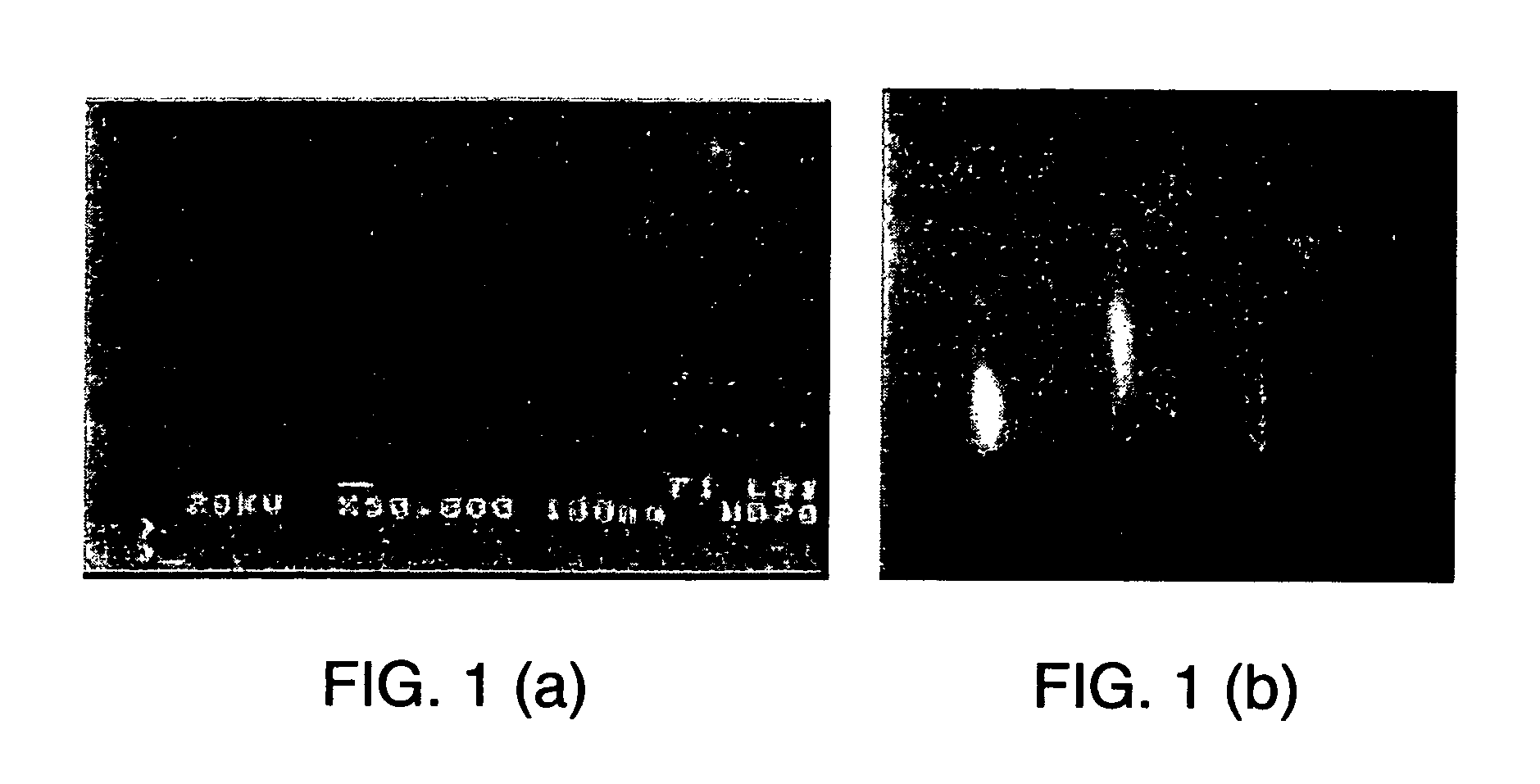
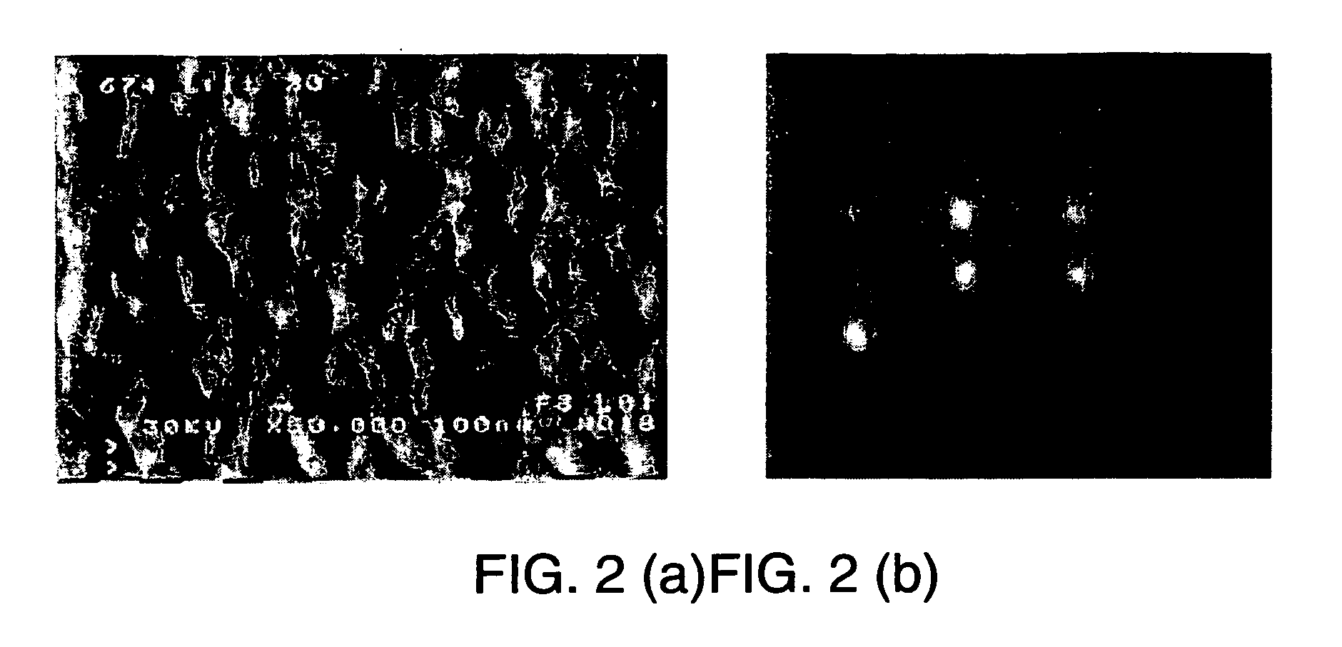
[0151]FIG. 21 shows a comparison of the photoluminescence lifetime in NCI AlGaN active region layers of present invention versus conventional AlGaN MQW (multiple quantum well) active region layers, deposited on both sapphire and a nitride semiconductor template. The conventional AlGaN MQW active region layers were designed for emission at 330 to 340 nm. They were deposited on a thin GaN template (buffer) on sapphire, and on a thick GaN HVPE free-standing substrate. The defect densities for the thin GaN template and the thick GaN substrate were estimated from etch pit counting by atomic force microscopy (AFM) to be ˜109 cm−2 and 107 cm−2, respectively.

[0152]It was found that the PL lifetime in the AlGaN MQW on the thin GaN template is about 100 ps, while for the AlGaN MQW on the thick GaN substrate the PL lifetime increases to about 500 ps (see G. A. Garrett, C. J. Collins, A. V. Sampath, H. Shen, M. Wraback, S. F. LeBoeuf, J. Flynn, and G. Brandes, Phys. Stat. Sol.(c) Vol. 2, No. 7,...


PUM


Abstract

An AlGaN composition is provided comprising a group III-Nitride active region layer, for use in an active region of a UV light emitting device, wherein light-generation occurs through radiative recombination of carriers in nanometer scale size, compositionally inhomogeneous regions having band-gap energy less than the surrounding material. Further, a semiconductor UV light emitting device having an active region layer comprised of the AlGaN composition above is provided, as well as a method of producing the AlGaN composition and semiconductor UV light emitting device, involving molecular beam epitaxy.

Description

[0001]This application claims the priority of the corresponding provisional application Ser. No. 60 / 663,144, filed Mar. 18, 2005, the entire contents of which are incorporated herein by reference. This application is related to application Ser. No. 11 / 376,452 filed on even date for a Method of Manufacturing An Ultraviolet Light Emitting AlGaN Composition And Ultraviolet Light Emitting Device Containing Same.STATEMENT OF GOVERNMENT INTEREST[0002]The invention described herein may be manufactured and used by or for the Government of the United States of America for governmental purposes without the payment of any royalties thereon or therefor.FIELD OF THE INVENTION[0003]The present invention provides an ultraviolet (UV) light emitting AlGaN composition, a UV light emitting device, and a method of making both. In particular, a UV light emitting device is provided comprised of an active region layer composed of AlGaN having localized nanoscale compositional inhomogeneities therein, as w...

Claims


Application Information

Patent Timeline
Patent Type & Authority Patents(United States)
IPC IPC(8): H01L21/28
CPCB82Y20/00H01L21/0254H01L21/02631H01L33/007H01S5/34333H01L21/0242H01L21/02458H01L21/02576H01S5/10H01S5/3209
Inventor SAMPATH, ANAND VENKTESHCOLLINS, CHARLES J.GARRETT, GREGORY ALANSHEN, H. PAULWRABACK, MICHAEL
Owner US SEC THE ARMY THE
Why Eureka
Try Eureka