Liquid crystal display device and method of manufacturing the same

a liquid crystal display and structure technology, applied in the manufacture of electrode systems, electric discharge tubes/lamps, instruments, etc., can solve the problems of insufficient fixing strength of bead spacers and prone to move into effective pixels, so as to prevent faulty display, reduce the rate of occurrence of defective products, and improve the bonding force of bead spacers to the substrate of liquid crystal display devices

Inactive Publication Date: 2010-10-12
PANASONIC LIQUID CRYSTAL DISPLAY CO LTD +1
View PDF29 Cites 6 Cited by
  • Summary
  • Abstract
  • Description
  • Claims
  • Application Information

AI Technical Summary

Benefits of technology

[0022]Thus, an object of the present invention is to provide a structure of a liquid crystal display panel in which the bead spacers, which should be disposed in the portions which do not affect the display quality and are located between the pixel regions, are prevented from moving to valid pixels to prevent the display quality from being affected while the liquid crystal display panel is being assembled, carried, or used, and a method of manufacturing the liquid crystal display panel using the bead spacers.
[0038]According to the present invention, the bonding force of the bead spacer to the substrate of the liquid crystal display device is improved, so the shifting of the bead spacer during the assembly, carrying, or use of the liquid crystal display device is suppressed. Therefore, the bead spacer disposed in a region which is located between pixel regions and does not affect the display quality (non-display portion) is prevented from moving into the pixel regions to prevent faulty display.
[0039]Even when a bead spacer which has been conventionally known is to be used, the bead spacer is bonded to the non-display portion of the principal surface of the substrate by an organic material film used for, for example, the alignment film. In this case, during a process of printing the alignment film to the principal surface of the substrate and drying the alignment film, a process of installing the liquid crystal display device including the substrate to a frame or the like, the carrying or use of the liquid crystal display device, or the like, the risk of the bead spacer being broken (elastically deformed) by an external force applied thereto significantly reduces. This may be because the alignment film or the organic material film which are used to hold the bead spacer to the principal surface of the substrate absorbs an external force applied to the bead spacer because of its flexibility. Therefore, a change in cell gap of the liquid crystal display device, which is caused by the deformation or breakage of the bead spacer, is suppressed to reduce the rate of occurrence of a defective product. The bead spacer supported by the organic material film absorbs the external force applied to the bead spacer by elastic deformation in a wide area, which is caused by a self-reaction force. Thus, a high-quality liquid crystal display device can be mass-produced at high yield.

Problems solved by technology

However, in the case of the above-mentioned method, the fixing strength of the bead spacers is still insufficient.
Alternatively, the bead spacers are liable to move into the effective pixels by vibration or the like during transportation or usage of the liquid crystal display panel.

Method used


Image

  • Liquid crystal display device and method of manufacturing the same
  • Liquid crystal display device and method of manufacturing the same
  • Liquid crystal display device and method of manufacturing the same

Examples


first embodiment

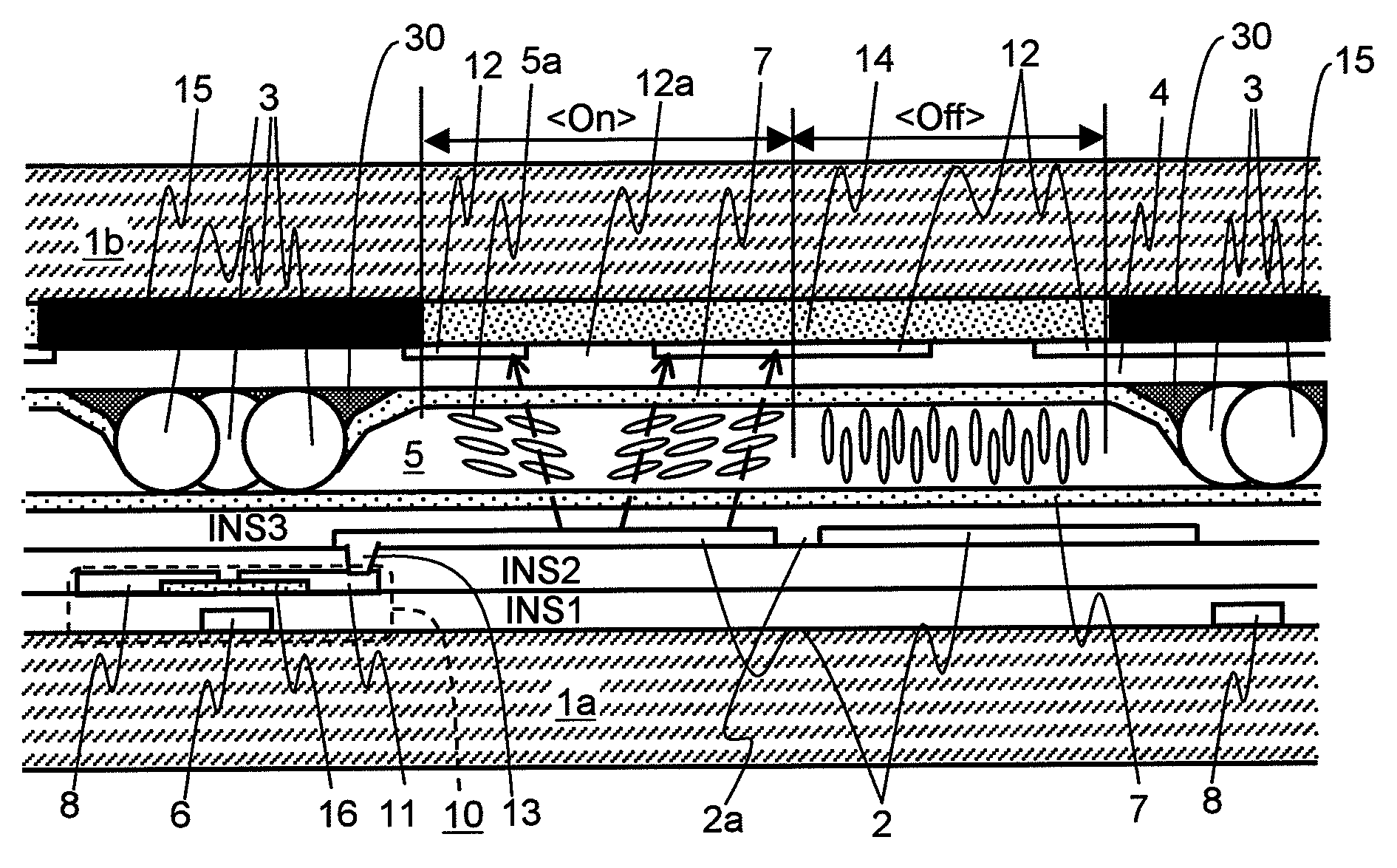
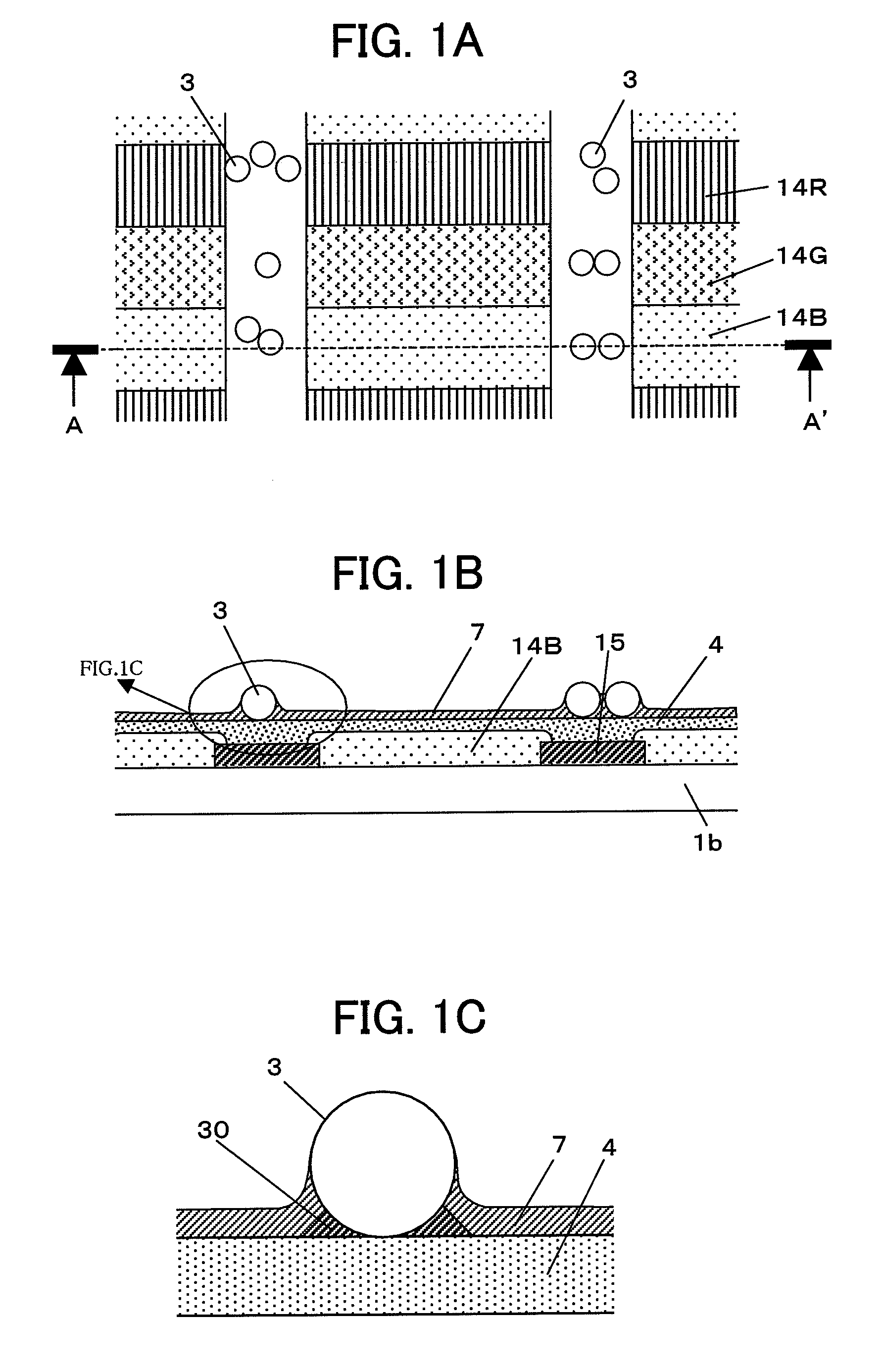
[0060]Principal constituent elements of a liquid crystal display device according to the present invention will be described in detail before the detailed descriptions of a structure of the liquid crystal display device according to the present invention and a method of manufacturing the same, to make features of the present invention clear, which will be described later.

Material of Bead Spacer 3

[0061]A spherical or cylindrical “piece (chip)” used as a spacer is made of an inorganic material such as silica or an organic material such as plastic. The piece made of the organic material is also called a plastic bead. In particular, the piece made of an organic polymer has a suitable hardness such that a resin layer, such as an alignment layer which is brought into contact therewith, is not damaged, easily follows a change in thickness which is caused by thermal expansion or thermal shrinkage, and has a relatively small movement inside the liquid crystal display device. The organic poly...

example 1

[0093]In order to prevent the shift of the bead spacers 3, according to the present invention, the surface tension of the high-boiling solvent contained in the spacer dispersion liquid is made higher than the surface tension of the precursor solution 7′ of the alignment film, so the bead spacers 3 are held to the light shielding region of the principal surface of the CF substrate 1b or the TFT substrate 1a by a residue of the spacer dispersion liquid. The spacer dispersion liquid landed on the principal surface of the substrate (CF substrate 1b) is evaporated to some extent before the precursor solution 7′ of the alignment film is applied to the principal surface thereof. A part of the spacer dispersion liquid is left on the principal surface of the substrate. The residue of the spacer dispersion liquid corresponds to the part of the spacer dispersion liquid left on the principal surface of the substrate immediately before the precursor solution 7′ is applied to the principal surfac...

example 2

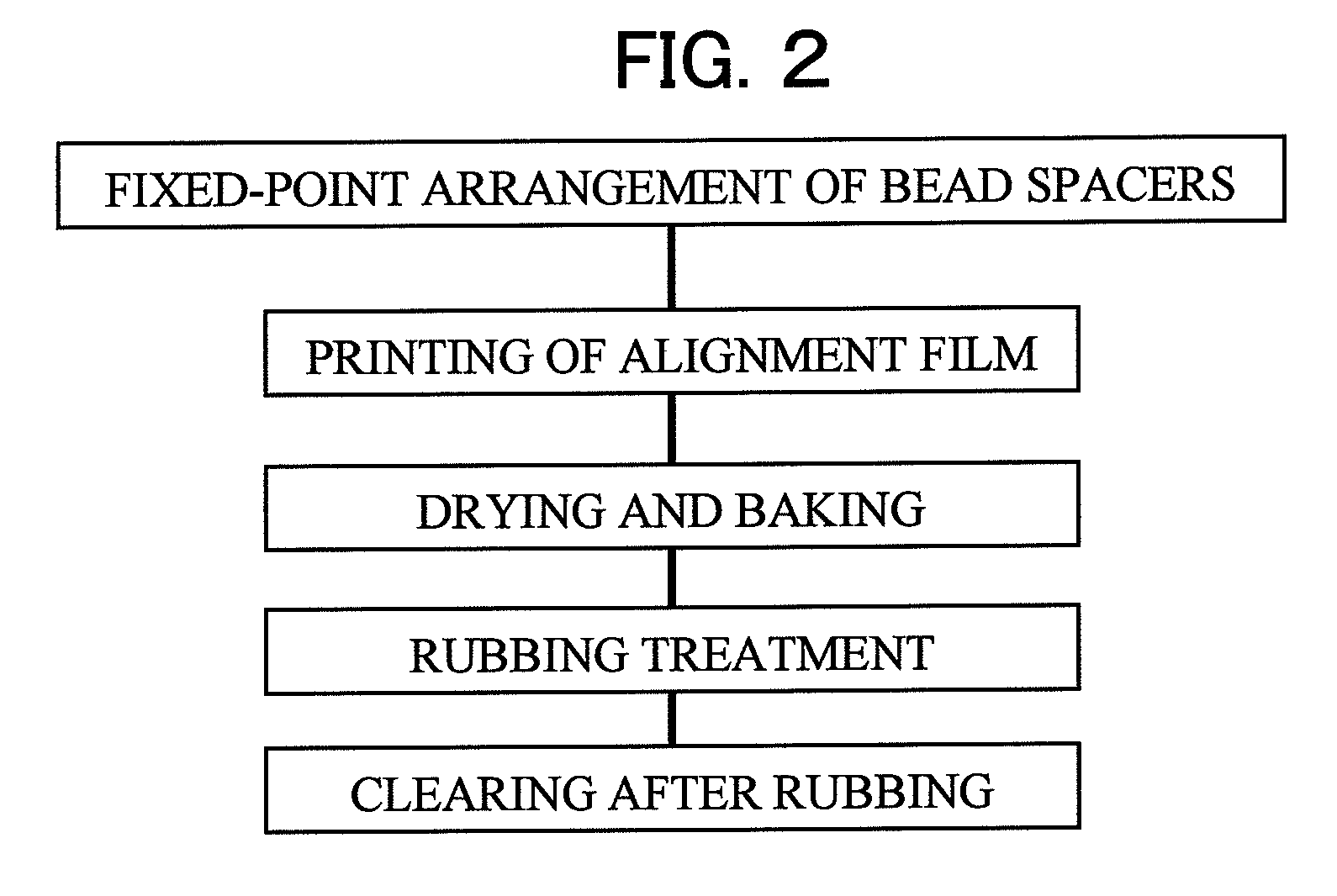
[0106]The following method will be described as another example to solve the technical problems with reference to FIGS. 7A to 7D. In this method, as shown in FIG. 6a, the alignment film 7 is disposed on the principal surface of the substrate (CF substrate 1b) and then the bead spacers 3 are disposed on the alignment film 7 (portions covering the light shielding film 15) by an ink jet method.

[0107]According to such a method, the bead spacers 3 are not moved by the precursor solution 7′ of the alignment film. However, the “shift of the bead spacers 3” which are dropped on the alignment film 7 (principal surface of the CF substrate 1b) or the “shift of the bead spacers 3” which is caused by the flow of a liquid crystal material injected to a space (cell gap) between the pair of substrates 1 bonded opposite to each other emerges as a new problem. The bead spacers 3 are in contact with the liquid crystal material, so the fixation of the bead spacers 3 to the alignment film 7 using an adh...


PUM

PropertyMeasurementUnit
viscosityaaaaaaaaaa
viscosityaaaaaaaaaa
surface tensionaaaaaaaaaa

Abstract

Bead spacers, which are disposed on at least one principal surface of a pair of substrates forming a liquid crystal display device, are bonded to the principal surface by an alignment film or an organic material film. Specifically, the bead spacers disposed on the principal surface are covered with the alignment film, or the bead spacers are bonded by the organic material film to the alignment film formed on the principal surface of the substrate.

Description

[0001]The present application claims priority from Japanese application JP 2007-034286 filed on Feb. 15, 2007, and Japanese application JP 2007-100023 filed on Mar. 6, 2007, the content of which is hereby incorporated by reference into this application.BACKGROUND OF THE INVENTION[0002]The present invention relates to a structure of a liquid crystal display device (liquid crystal display panel) and a method of manufacturing the liquid crystal display device, and more particularly, to optimization of an arrangement of bead spacers forming a space between a pair of substrates included in the liquid crystal display device.[0003]As shown in FIG. 9, a liquid crystal display panel (liquid crystal display device) 9 is constructed as described below, in which a liquid crystal layer 5 is sandwiched between a pair of (two) substrates typified by a thin film transistor (TFT) substrate 1a, on which thin film transistor is formed and a color filter (CF) substrate 1b on which red, blue, and green ...

Claims


Application Information

Patent Timeline
Patent Type & Authority Patents(United States)
IPC IPC(8): G02F1/1337G02F1/1339
CPCG02F1/13392G02F1/13394
Inventor KAWABE, SHINICHIHONOKI, HIDEYUKITANAKA, YUICHIRO
Owner PANASONIC LIQUID CRYSTAL DISPLAY CO LTD
Why Eureka
Try Eureka