Method and apparatus for analyzing defect data and a review system

a technology of defect data and review system, applied in the direction of mechanical roughness/irregularity measurement, image enhancement, instruments, etc., to achieve the effect of high speed

Active Publication Date: 2010-10-12
HITACHI HIGH-TECH CORP
View PDF11 Cites 30 Cited by
  • Summary
  • Abstract
  • Description
  • Claims
  • Application Information

AI Technical Summary

Benefits of technology

[0007]It is therefore an object of the present invention to provide a defect data analysis method and device and a review system capable of coping with a weak defect distribution pattern and outputting information supporting to identify a failure cause at a high speed without requiring user definitions.

Problems solved by technology

Most of defect distribution deflection is caused by a device failure or a process error.

Method used


Image

  • Method and apparatus for analyzing defect data and a review system
  • Method and apparatus for analyzing defect data and a review system
  • Method and apparatus for analyzing defect data and a review system

Examples


first embodiment

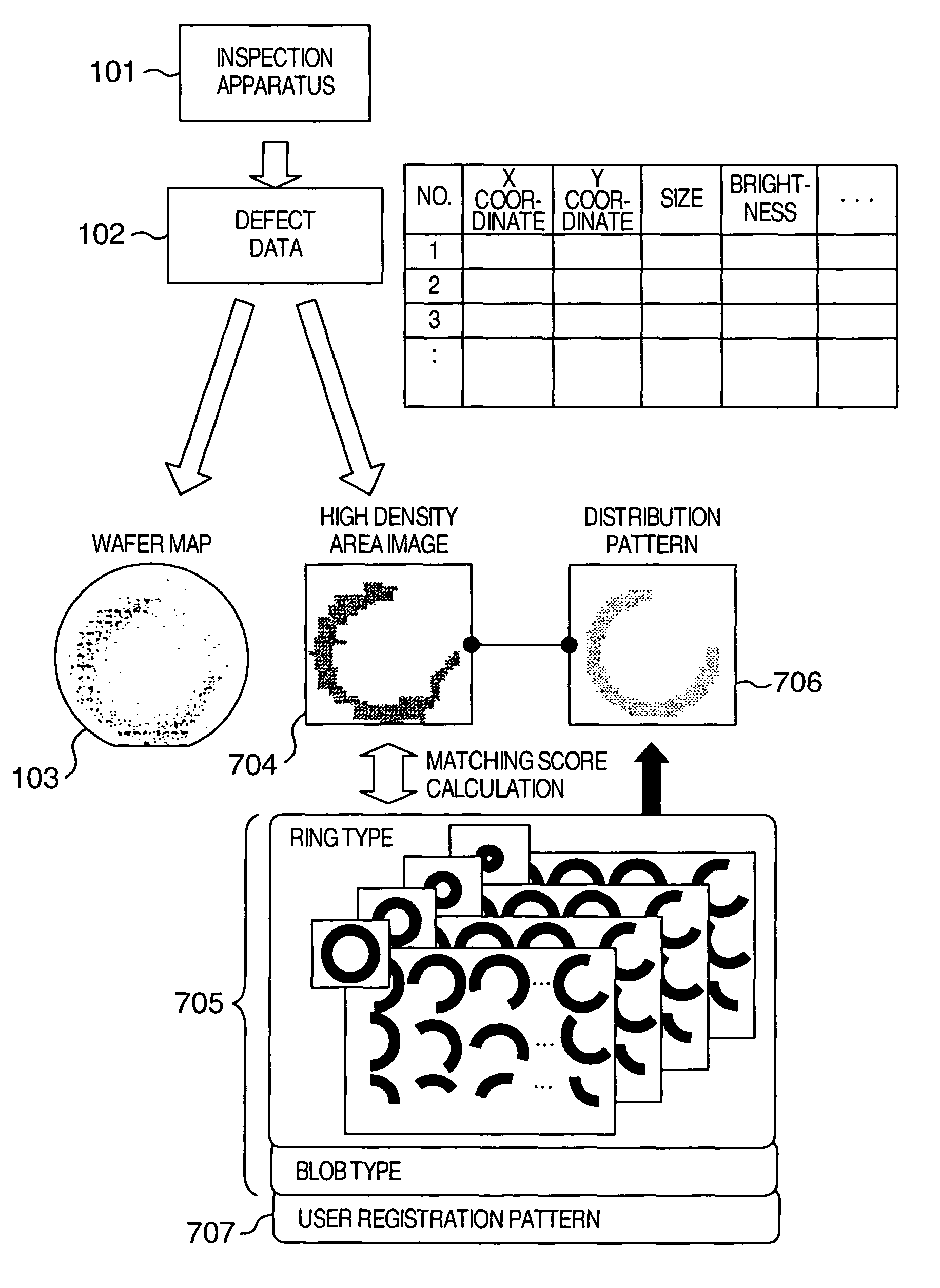
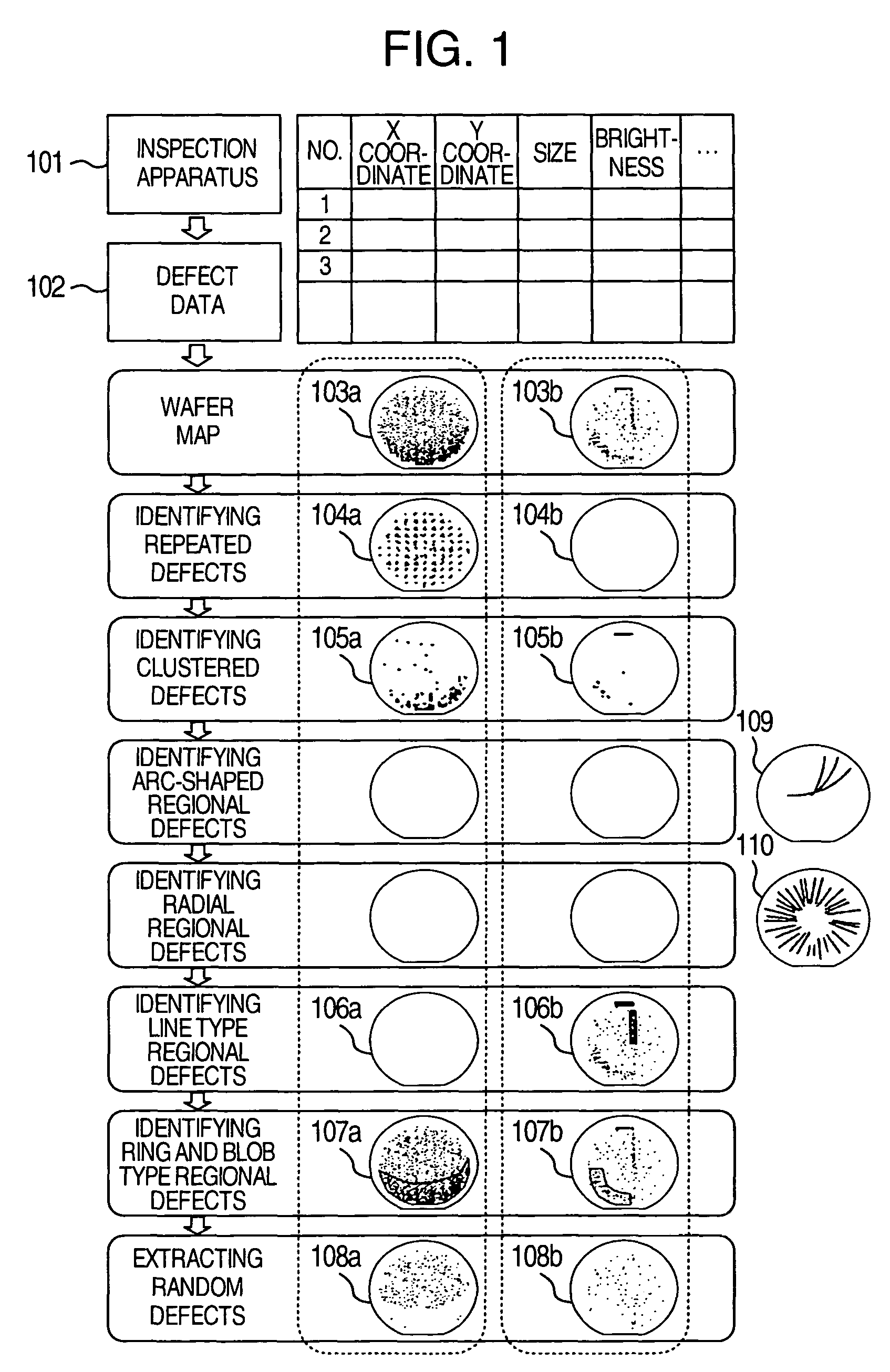
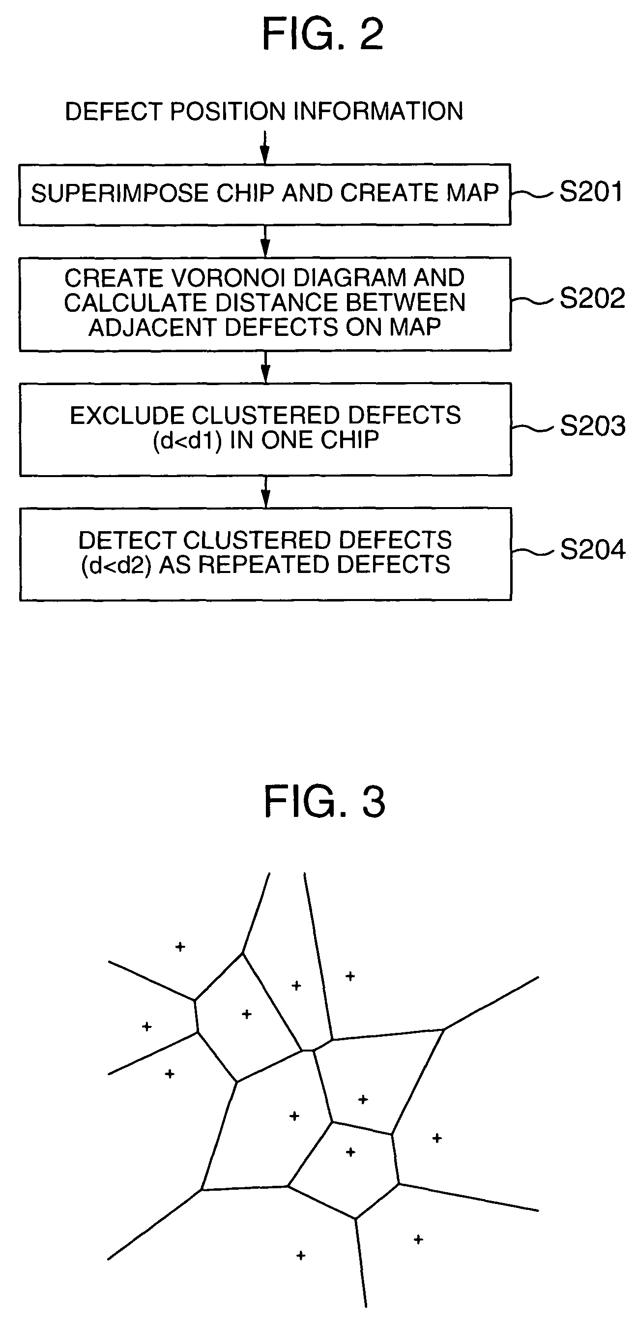
[0034]In the defect data analysis method according to the present invention, defect data 102 output from a semiconductor wafer inspection apparatus 101 includes at least position coordinates of defects. 103a and 103b are wafer maps showing the defect positions on a coordinate system having one point on the waver as an origin. The defect position coordinates output from the inspection apparatus may be described by a coordinate system having one point on the wafer as an origin or a coordinate system having an origin for each chip. In the former case, X and Y coordinate values are directly used while in the latter case, the position coordinates in the chip should be converted into another coordinate system by using the chip arrangement information and the chip size information. According to the defect distribution state on the wafer map, defects are classified into the following defect distribution characteristic categories: repeated defects, clustered defects, arc-shaped regional defe...

second embodiment

[0109]FIG. 20 shows configuration of the inspection apparatus according to the present invention.

[0110]The pattern information addition means 301 adds a sampling condition number in addition to the aforementioned information. By manually grouping the template patterns using the same sampling condition, the same sampling number is added. When no sampling condition is present corresponding to the number, a sampling condition is created by sampling condition creation means 307.

[0111]The sampling condition creation means 307 creates a sampling condition to decide a defect for performing review. The sampling condition related to the ring and blob type regional defect pattern and sampling conditions of other distribution characteristic categories are manually created and stored as a sampling condition file 312 in the storage means 302. The sampling condition may be, for example, the sampling count or the sampling ratio and sampling method. The sampling count or the sampling ratio is selec...


PUM

PropertyMeasurementUnit
defect data analysisaaaaaaaaaa
defect positionaaaaaaaaaa
defect distributionaaaaaaaaaa

Abstract

In a process for manufacturing a semiconductor wafer, defect distribution state analysis is performed so as to facilitate identification of the defect cause including a device cause and a process cause by classifying the defect distribution state according to the defect position coordinates detected by the inspection device, into one of the distribution characteristic categories: repeated defects, clustered defects, arc-shaped regional defects, radial regional defects, line type regional defects, ring and blob type regional defects, and random defects.

Description

BACKGROUND OF THE INVENTION[0001]The present invention relates to a defect data analyzing method and apparatus and a review system for analyzing defect distribution state from defect data detected by an inspection apparatus in a semiconductor wafer manufacturing process.[0002]In a semiconductor device manufacturing procedure forming a circuit pattern on a semiconductor substrate (hereinafter, referred to a semiconductor wafer manufacturing procedure), a pattern defect inspection or a foreign matter inspection is performed after each process and inspection result is analyzed, so as to improve the yield and stability. As one of such methods, a defect distribution state analysis is known. Most of defect distribution deflection is caused by a device failure or a process error. For this, it is tried to identify a defect cause by identifying a defect distribution pattern characteristic to a device failure or a process error.[0003]There are conventional techniques concerning this as follow...

Claims


Application Information

Patent Timeline
Patent Type & Authority Patents(United States)
IPC IPC(8): G06K9/00G01B11/24G01B5/28G01N21/956G06T7/00H01L21/02
CPCG06T7/0004G06T2207/30148
Inventor SHIBUYA, HISAETAKAGI, YUJI
Owner HITACHI HIGH-TECH CORP
Why Eureka
Try Eureka