LED package structure and manufacturing method, and LED array module

a technology of led array modules and package structures, which is applied in the direction of electrical equipment, semiconductor devices, semiconductor/solid-state device details, etc., can solve the problems of poor thermal radiation, exponential decay of led performance, and high power consumption of led backlight units used in lcd backlight units or lighting apparatuses, etc., to achieve excellent thermal radiation performance, high power led package, and low cost

Inactive Publication Date: 2010-10-26
SAMSUNG ELECTRONICS CO LTD
View PDF9 Cites 16 Cited by
  • Summary
  • Abstract
  • Description
  • Claims
  • Application Information

AI Technical Summary

Benefits of technology

[0015]Accordingly, it is one exemplary object of the present invention to provide a light emitting diode (LED) package having excellent thermal radiation performance and which is suitable for a high power LED package, and low cost a manufacturing method thereof.

Problems solved by technology

LEDs used in backlight units for LCDs or in lighting apparatuses require high power consumption.
However, when the temperature rises, the performance of an LED exponentially decays.
However, this conventional LED package above has a relatively long heat transfer path (i.e. LED→insulating layer→heat sink member→solder→substrate), so that it has poor thermal radiation due to an increase in thermal resistance.
Accordingly, it is not suitable for a high power LED package.
When an LED package has poor thermal radiation performance, the lifetime of the LED is decreased and peripheral parts near the LED package may deteriorate or become thermally deformed because of the heat, thus possibly causing system damage.
Additionally, such a conventional LED package requires a separate wire bonding process and when such an LED is added to an LED array module, a lengthy process of soldering a plurality of packages is required, thereby increasing the number of assembly processes required and also increasing manufacturing costs.

Method used


Image

  • LED package structure and manufacturing method, and LED array module
  • LED package structure and manufacturing method, and LED array module
  • LED package structure and manufacturing method, and LED array module

Examples


Embodiment Construction

[0065]Hereinafter, a light emitting diode (LED) package, a manufacturing method thereof, and an LED array module using the same according to exemplary embodiments of the present invention will be described in detail with reference to the accompanying drawings. In the description, if it is determined that a detailed explanation of related known functions or constructions makes the gist of the invention ambiguous, it will be omitted.

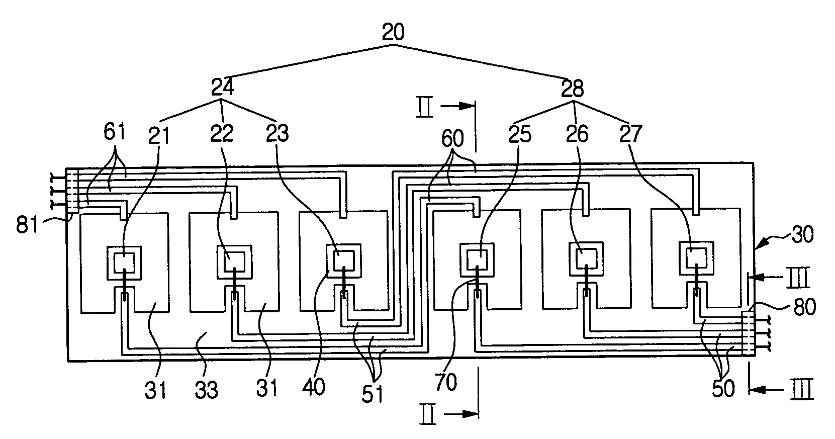
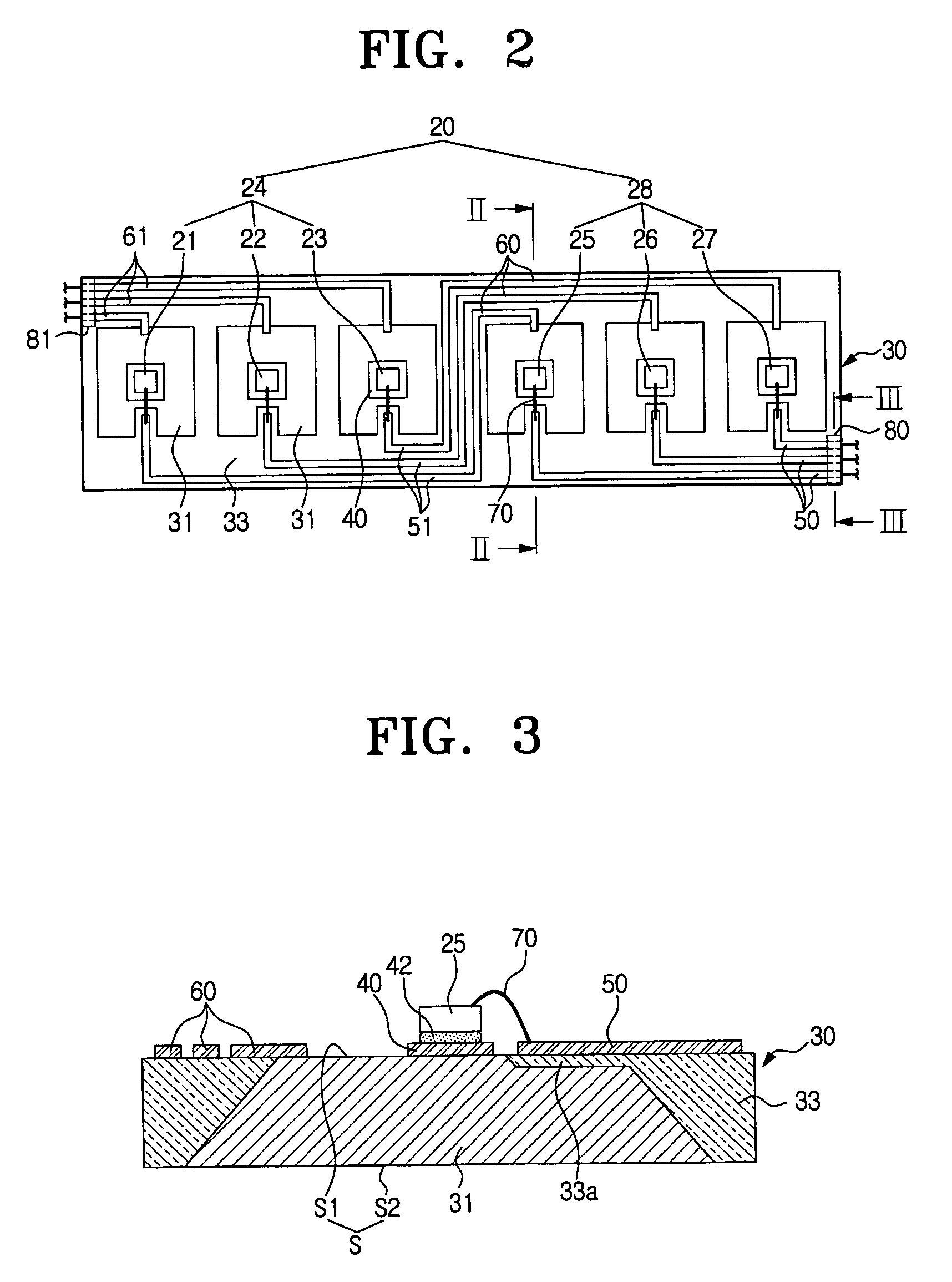
[0066]As illustrated in FIG. 2, an LED array module according to a first exemplary embodiment of the invention includes a plurality of LEDs 20, a substrate 30 mounting thereon the LEDs 20, a plurality of base electrodes provided on the upper portion of the substrate 30, a first electrode 50, and a second electrode 60.

[0067]Herein, the plurality of LEDs 20 consist of a plurality of LED units 24 and 28, each having at least one of R LED 21 or 25, G LED 22 or 26, and B LED 23 or 27, respectively, emitting red light, green light and blue light, respectively. T...


PUM


Abstract

An LED package includes a substrate having an electrically conductive portion and an electrically non-conductive portion composed of an oxide of the conductive portion; an LED mounted on the conductive portion and electrically connected to the conductive portion; a first electrode disposed on the non-conductive portion and electrically connected to the LED by a wire; and a second electrode disposed on the substrate and electrically connected to the LED.

Description

CROSS-REFERENCE TO RELATED APPLICATIONS[0001]This application claims priority under 35 U.S.C. §119 from Korean Patent Application No. 2005-69519, filed on Jul. 29, 2005, the entire content of which is incorporated herein by reference.BACKGROUND OF THE INVENTION[0002]1. Field of the Invention[0003]Methods and apparatuses consistent with the present invention relate to a light emitting diode (LED) package usable for a backlight unit, such as a liquid crystal display (LCD), or a lighting apparatus, a manufacturing method thereof, and an LED array module using the same.[0004]2. Description of the Related Art[0005]Light emitting diodes (LEDs) have been widely used in many fields, including electronics and advertising, due to their long life and their low power consumption. Recently, there have been attempts to use LEDs as backlight units for LCD devices, and in the future, LEDs may also be widely used in common lighting systems. Therefore, there is an increasing demand for small LED pack...

Claims


Application Information

Patent Timeline
Patent Type & Authority Patents(United States)
IPC IPC(8): H01L29/74H01L33/64H01L33/62
CPCH01L33/647H01L25/0753H01L33/486H01L33/62H01L33/642H01L2224/32188H01L2224/48091H01L2224/48247H01L2224/73265H01L2924/01078H01L2924/01079H01L2924/00014H01L2224/32245H01L2924/01019H01L2924/00H01L2924/12041
Inventor SHIN, SU-HOKWEON, SOON-CHEOLSHIN, KYU-HOKWON, KI-HWANCHOI, SEUNG-TAEMOON, CHANG-YOUL
Owner SAMSUNG ELECTRONICS CO LTD
Why Eureka
Try Eureka