CMOS device with zero soft error rate

a technology of soft error rate and cmos device, which is applied in the direction of semiconductor devices, electrical apparatus, transistors, etc., can solve the problems of soft error rate, integrated circuit reliability, soft error rate (james f. ziegler), soft error rate, etc., and achieve the effect of eliminating soft errors without added cos

Inactive Publication Date: 2010-10-26
AVOLARE 2 LLC
View PDF13 Cites 7 Cited by
  • Summary
  • Abstract
  • Description
  • Claims
  • Application Information

AI Technical Summary

Benefits of technology

[0022]One of the advantages of the present invention is that it eliminates parasitic bipolar action and dramatically reduces the field-funneling effect. As a result, a CMOS device in accordance with the principles of the present invention is unconditionally immune to latch-up, snapback effects, single-event latchup (SEL), single-event upset (SEU), and multi-bit upsets (MBU), thereby having zero soft error rate.

Problems solved by technology

One type of integrated circuit reliability problem known in the art is soft errors (James F. Ziegler, “SER—History, Trends and Challenges.
Soft errors occur when digital information spontaneously changes due to radiation effects.
Soft errors do not permanently damage hardware but rather corrupt electronically stored information, which can lead to circuit failure.
High energy neutrons tend to be the most problematic radiation source as they are difficult to absorb by packaging techniques, and following a nuclear reaction between the incident neutron and a silicon atom in the substrate, secondary ions are produced that generate approximately ten times as much free charge compared to the charge generated from an alpha particle strike (Kenichi Osada et al., “Analysis of SRAM Neutron-Induced Errors Based on the Consideration of Both Charge-Collection and Parasitic-Bipolar Failure Modes,” IEEE 2004 Custom Integrated Circuits Conference, p.
The device may be part of a larger cell or integrated circuit such as a 6-T SRAM cell that comprises two cross-coupled CMOS devices, and which is particularly susceptible to soft errors.
Furthermore, the floating P-well 120 activates a parasitic bipolar device between the P-well 120 and the neighboring cell (not shown), which leads to a flow of back-injected electrons from the neighboring cell source to the neighboring cell drain, and therefore a lowering of the voltage on the neighboring cell drain and ultimately a soft error.
Latch-up is unique problem for CMOS circuits and is caused by the presence of lateral bipolar NPN and PNP transistors.
These unwanted parasitic bipolar transistors can act as amplifiers, causing the circuit to fail by shorting power to ground.
However, these approaches generally do not guarantee elimination of the soft error problem and are used at the expense of added cost, size, weight, and generally decreased speed performance and increased power consumption.
Furthermore, as semiconductor technology continues to scale to higher density integration, lower storage node capacitances and reduced voltages, integrated circuits become increasingly sensitive to the radiation effects that cause soft errors.
As a result, the problem of soft errors will become an increasingly problematic reliability challenge for integrated circuit manufacturers in the future.

Method used


Image

  • CMOS device with zero soft error rate
  • CMOS device with zero soft error rate
  • CMOS device with zero soft error rate

Examples


Embodiment Construction

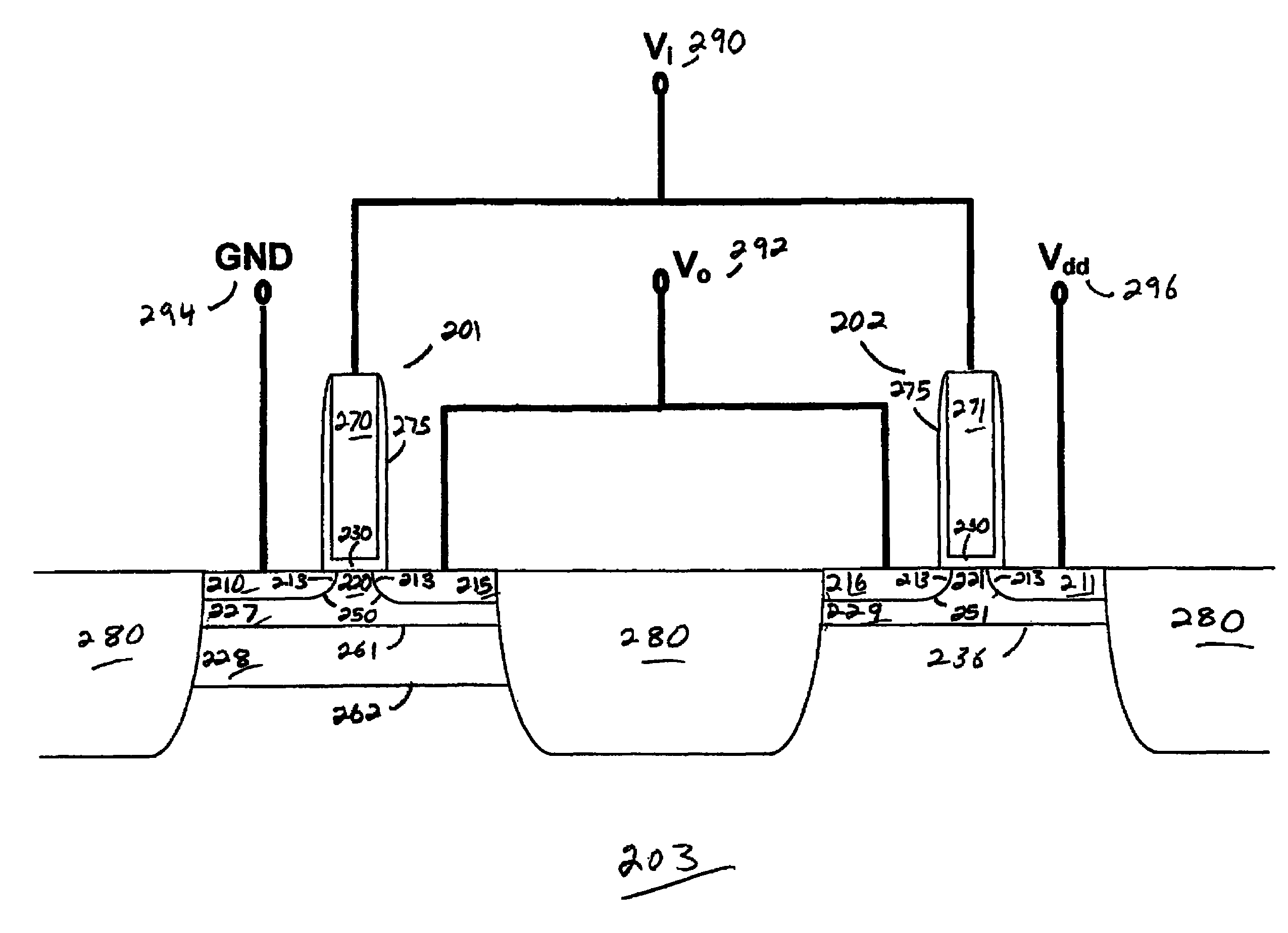
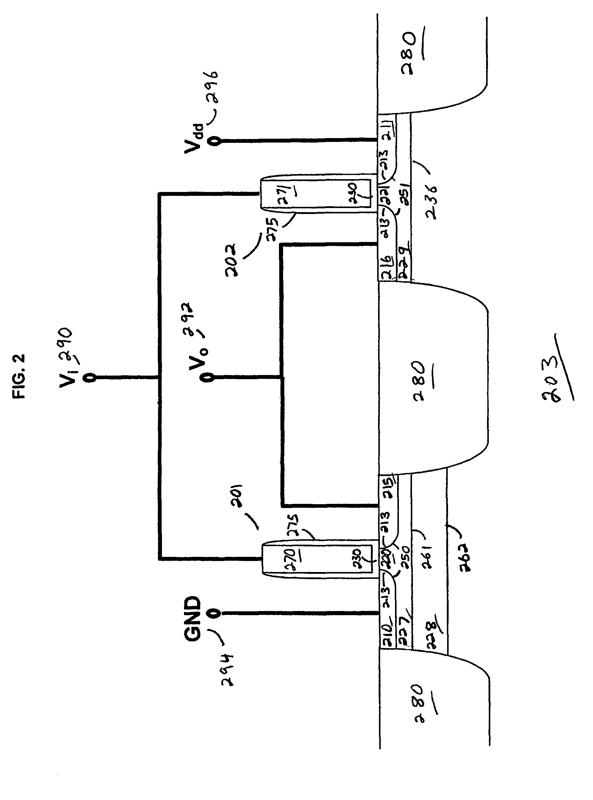
[0021]In general, the present invention provides an integrated circuit and method of fabrication, the circuit having zero soft error rate. In one embodiment of the present invention, the integrated circuit is generally comprised of at least one NMOS device or at least one PMOS device; wherein at least one of the NMOS devices or PMOS devices is a Schottky barrier MOS (SB-MOS) device with no parasitic bipolar action and significantly reduced field-funneling effect during an energetic particle strike by means of a buried well structure. The present invention also provides a method comprising the steps of providing a semiconductor substrate; providing isolation regions, such as STI, that separate NMOS active regions and PMOS active regions; providing an N-type well (N-well) implant in the NMOS active region and a P-type well (P-well) implant in the NMOS active region, the first N-well located vertically below the P-well region; providing a second N-well implant in the PMOS active region...


PUM


Abstract

A CMOS device and method of manufacture is provided for producing an integrated circuit that is not susceptible to various soft errors such as single-event upsets, multi-bit upsets or single-event latchup. The CMOS device and method utilizes a new and novel well architecture in conjunction with metal source / drain electrodes to eliminate soft errors. In one embodiment, the CMOS device uses a first metal source / drain material for the NMOS device and a second metal source / drain material for the PMOS device. The CMOS device further uses a multi-layered well-structure with a shallow N-well and a buried P-well for the PMOS device and a shallow P-well and a buried N-well for the NMOS device.

Description

CROSS-REFERENCE TO RELATED APPLICATION[0001]This application claims the benefit of and priority to U.S. provisional patent application Ser. No. 60 / 726,042, filed Oct. 12, 2005.FIELD OF THE INVENTION[0002]The present invention generally relates to the field of semiconductor systems and manufacturing processes. More particularly, the present invention relates to semiconductor integrated circuits (ICs) having transistors for regulating the flow of electric current having metal sources and / or drains forming Schottky or Schottky-like contacts to a channel region, and the manufacturing processes thereof.BACKGROUND OF THE INVENTION[0003]One type of integrated circuit reliability problem known in the art is soft errors (James F. Ziegler, “SER—History, Trends and Challenges. A Guide for Designing with Memory ICs”). Soft errors occur when digital information spontaneously changes due to radiation effects. Soft errors do not permanently damage hardware but rather corrupt electronically stored ...

Claims


Application Information

Patent Timeline
Patent Type & Authority Patents(United States)
IPC IPC(8): H01L27/095H01L27/092H01L21/8238
CPCH01L21/823814H01L21/823892H01L27/0921H01L29/66636H01L29/66643H01L29/7839
Inventor SNYDER, JOHN P.LARSON, JOHN M.
Owner AVOLARE 2 LLC
Why Eureka
Try Eureka