Fingerprint sensor using a spectral filter and a holographic optical element
a holographic optical element and fingerprint sensor technology, applied in the field of fingerprint sensor using a spectral filter and holographic optical element, can solve the problems of image laterally shifted with respect to the actual finger, aberration, and insufficient light transmission band of the filter, so as to avoid the use of expensive optics, avoid aberration, and avoid astigmatism.
- Summary
- Abstract
- Description
- Claims
- Application Information
AI Technical Summary
Benefits of technology
Problems solved by technology
Method used
Image
Examples
first embodiment
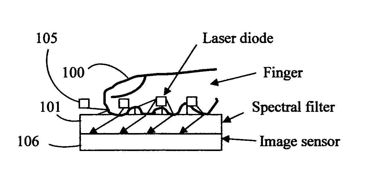
[0022]FIG. 3a shows an example of the optical configuration of the invention. It includes a sensing surface which is the top surface of the spectral filter 101. The element 102 is a special holographic grating designed to converge oblique incident rays. It is needed to gather information from all the ridges and transmit it to the camera lens. It is basically a transmission hologram of a spherical wavefront and a collimated slanted beam of light. When such a hologram is illuminated by antiparallel collimated beam, the result is a focused spot. The element 103 is a transparent slab of appropriate thickness and serves as a support for the two elements 101 and 102. The thickness is chosen to avoid ghost images due to internal reflections within the element. FIG. 3b shows the top view of the unit. Element 105 is a set of narrow band sources for illumination of the finger 100. Element 104 is the lens system and could comprise of several lenses. Element 106 is an image sensor such as a CCD...
second embodiment
[0024]FIG. 5 shows the invention. A thin band pass interference filter 101, a thin holographic optical grating 102 and the image sensor 106 are cemented together to form a compact fingerprint sensor. In case an ideal filter 101 is not available, then a blocking band pass filter matched to the center wavelength of the source 105 is sandwiched between the holographic grating and the image sensor as shown in FIG. 6. Filter 107 would essentially block most of the room light while transmitting the source wavelengths. The elements 101, 102 and 107 must be as thin as possible for sharp imaging.
[0025]FIG. 7 shows the simplest design of a fingerprint device. It consists of a coating of an interference band pass filter over the image sensor. The central wavelength of the narrowband source is shifted with respect to the center of the pass band of the filter. This combination leads to yet another compact fingerprint sensor. A properly designed band pass filter in the form of a thin coating can ...
PUM
 Abstract
Description
Claims
Application Information


