Fingerprint sensor using a spectral filter and a holographic optical element

a holographic optical element and fingerprint sensor technology, applied in the field of fingerprint sensor using a spectral filter and holographic optical element, can solve the problems of image laterally shifted with respect to the actual finger, aberration, and insufficient light transmission band of the filter, so as to avoid the use of expensive optics, avoid aberration, and avoid astigmatism.

Inactive Publication Date: 2009-05-07
BAHUGUNA RAMENDRA DEO
View PDF7 Cites 24 Cited by
  • Summary
  • Abstract
  • Description
  • Claims
  • Application Information

AI Technical Summary

Benefits of technology

[0008]Igaki et. al. (Applied Optics, Vol. 31, pp. 1794-1802 (1992)) came up with a sensor that was based on total internal reflection. In their method, light from the valleys of the finger can only be seen within a cone whose angle is the critical angle in the sensor material. Light from ridges, however, is scattered in all directions. To separate the information of ridges from the valleys, i.e. for good contrast, only the rays at an angle greater than the critical angle are collected. This way the rays from the valleys are avoided. The rays from the ridges are then bent by a holographic grating and focused by a camera. This way the final image is projected normal to the camera. The image, however, is laterally shifted with respect to the actual finger and aberrated with astigmatism principally caused by the holographic grating. Expensive optics is needed to correct the aberrations. When the distance between the hologram and an object to be detected is shortened in a hologram reconstruction mode, aberrations can be eliminated which is what has been achieved in the invention described below. In fact the distance has been reduced to few microns in one of the embodiments. This has been made possible by using the fact that in a spectral band pass interference filter the pass band shifts with change in the angle of incidence of the incoming light ray.
[0009]The present invention makes it possible to see the image in a direction normal to the finger with no significant lateral shift thus avoiding the use of expensive optics. It is based on the fact that the central wavelength of the transmission band of a narrow band interference filter depends on the angle of incidence, and shifts to shorter wavelengths as the angle of incidence is increased. FIG. 4 illustrates the principle of operation. As an example, let us shine the finger with light at 635 nm and select a filter whose bandpass is centered at 728 nm and designed for normal incidence. The light at a shorter wavelength such as 635 nm, scattered from the valleys is confined within the critical angle, say 420, of the filter medium. Even at 420 the shift in the transmission band of the filter is not enough to allow light at 635 nm to get through. Hence the light from the valleys is blocked by the spectral filter and is not collected by the camera. The light from the ridges is scattered in all directions. Light from the ridges around say 450, shifts the central band of the spectral filter very close to 635 nm, thus allowing the light to be transmitted by the filter. The transmitted rays which originate from the ridges are then bent and focused by the holographic optical element towards the camera. Thus the valleys appear dark and the ridges appear bright leading to a high contrast fingerprint image. The numbers used in the above example are for illustration only. A prototype using numbers which were close to the one discussed above has been built and works well. Exact calculations can be made for spectral shifts vs. angle of incidence and a fingerprint device built with any narrow interference band pass filter with the appropriate wavelength of the light source.
[0010]The above sensor shown in FIG. 3 (and FIG. 4) can be miniaturized by directly coating a holographic emulsion on an image sensor and creating the holographic optical element in it. The spectral filter can then be directly fabricated over the hologram. This way the use of lens and glass slab is avoided, leading to a miniature sensor. In this case the holographic optical element is not a converging one and simply bends the inclined rays from the ridges in a direction normal to the image as shown in FIG. 5. The spectral filter and the holographic emulsion are very thin (several micrometers.)

Problems solved by technology

The image, however, is laterally shifted with respect to the actual finger and aberrated with astigmatism principally caused by the holographic grating.
Even at 420 the shift in the transmission band of the filter is not enough to allow light at 635 nm to get through.

Method used


Image

  • Fingerprint sensor using a spectral filter and a holographic optical element
  • Fingerprint sensor using a spectral filter and a holographic optical element
  • Fingerprint sensor using a spectral filter and a holographic optical element

Examples


first embodiment

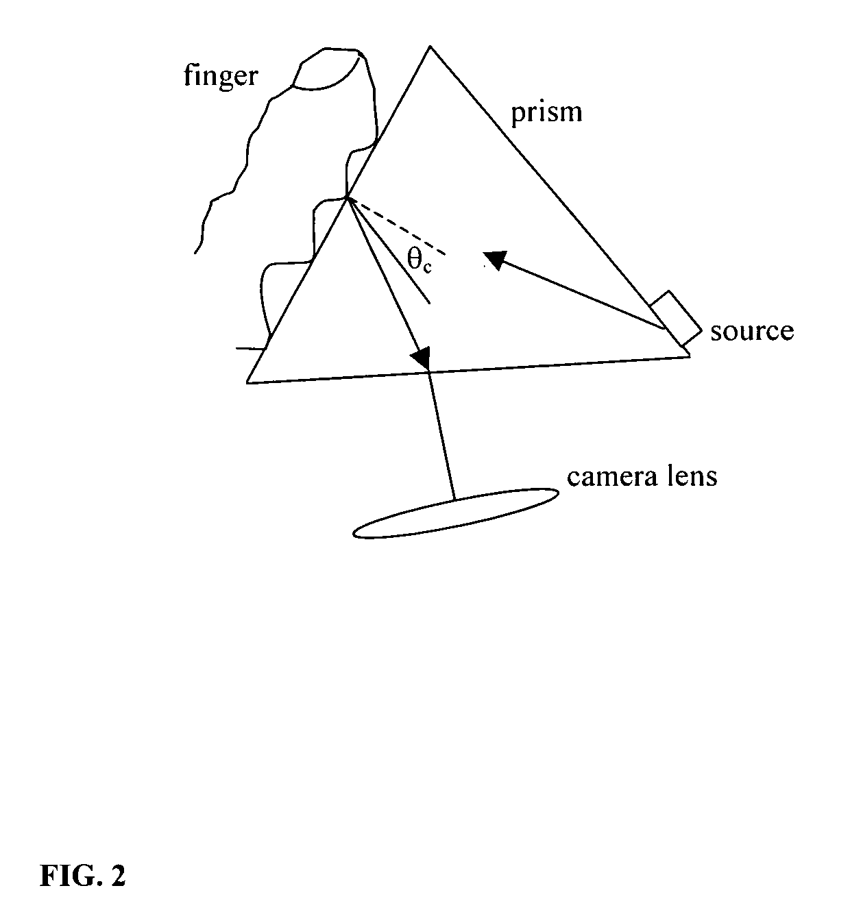
[0021]FIG. 3a shows an example of the optical configuration of the invention. It includes a sensing surface which is the top surface of the spectral filter 101. The element 102 is a special holographic grating designed to converge oblique incident rays. It is needed to gather information from all the ridges and transmit it to the camera lens. It is basically a transmission hologram of a spherical wavefront and a collimated slanted beam of light. When such a hologram is illuminated by antiparallel collimated beam, the result is a focused spot. The element 103 is a transparent slab of appropriate thickness and serves as a support for the two elements 101 and 102. The thickness is chosen to avoid ghost images due to internal reflections within the element. FIG. 3b shows the top view of the unit. Element 105 is a set of narrow band sources for illumination of the finger 100. Element 104 is the lens system and could comprise of several lenses. Element 106 is an image sensor such as a CCD...

second embodiment

[0023]FIG. 5 shows the invention. A thin band pass interference filter 101, a thin holographic optical grating 102 and the image sensor 106 are cemented together to form a compact fingerprint sensor. In case an ideal filter 101 is not available, then a blocking band pass filter matched to the center wavelength of the source 105 is sandwiched between the holographic grating and the image sensor as shown in FIG. 6. Filter 107 would essentially block most of the room light while transmitting the source wavelengths. The elements 101, 102 and 107 must be as thin as possible for sharp imaging.

[0024]FIG. 7 shows the simplest design of a fingerprint device. It consists of a coating of an interference band pass filter over the image sensor. The central wavelength of the narrowband source is shifted with respect to the center of the pass band of the filter. This combination leads to yet another compact fingerprint sensor. A properly designed band pass filter in the form of a thin coating can ...


PUM


Abstract

In one embodiment, a fingerprint sensing system includes a interference narrow band pass filter, a holographic optical element, a transparent slab stacked together with optical cement. The finger is placed on the filter and illuminated by a narrow band source, the center of its band shifted appropriately with respect to the pass band of the interference filter. A camera on the other side of the slab receives the fingerprint image. The light from the valleys and ridges propagating in the direction of the camera are blocked by the interference filter. The light from the ridges at steep angles are bent by the holographic optical element and then directed towards the lens. This way the ridges are seen by the camera, but not the valleys. In another embodiment, a miniaturized version, the interference filter, a modified holographic optical element, and a blocking filter (if necessary) to block room light can be sequentially attached to the image sensor. In yet another embodiment, the interference filter can be directly coated over an image sensor creating a very simple fingerprint sensor. The principle behind all of the above embodiments is the same, viz: the spectral transmission band of an interference filter shifts with change in the angle of incidence.

Description

1. BACKGROUND OF THE INVENTION[0001]1. Field of Invention[0002]This invention relates to acquisition of fingerprints and other relieved-surface images via optical means. This invention relates more particularly to the use of total internal reflection and spectral shift of the transmission band in Interference filters due to change in the angle of incidence.[0003]2. Prior Art[0004]Optical fingerprint sensors are usually based on total internal reflection of light. The principle of total internal reflection can be applied in two different ways to create a sensor. The first kind is an absorptive sensor and the second one is scattering-type.2.1. Absorptive Sensor[0005]The finger is placed on the surface of a glass prism and light is incident through another face of the prism. The angle of incidence is greater than the critical angle and hence all of the light is totally internally reflected from the valleys of the finger. The ridges, however, absorb most of the light. This way the valle...

Claims


Application Information

Patent Timeline
Patent Type & Authority Applications(United States)
IPC IPC(8): G01B9/021
CPCG06K9/00046G06V40/1324
Inventor BAHUGUNA, RAMENDRA DEO
Owner BAHUGUNA RAMENDRA DEO
Why Eureka
Try Eureka