Current-injecting/tunneling light-emitting device and method

a current injection/tunnel technology, applied in the field of semiconductor light emitters and devices, can solve problems such as waste of energy, heat conversion, waste of energy,

Active Publication Date: 2010-11-30
LIGHTWAVE PHOTONICS INC
View PDF5 Cites 15 Cited by
  • Summary
  • Abstract
  • Description
  • Claims
  • Application Information

AI Technical Summary

Problems solved by technology

Despite the significant resources expended to develop and commercialize group III-nitride based light-emitting devices significant difficulties and barriers still exist to realizing group III-nitride based light-emitting devices with improved efficiency, reliability and performance characteristics.
The initial drop in energy of the electron from the bottom of the n-type conduction band to the energy potential of the sub-band minimum of the active region is converted into heat and therefore wasted energy.
This wasted energy is an issue because the generation of heat is not desirable due to decreased device reliability, and LEDs that are efficient in converting electrical energy to light are favored.
Moreover, in conventional LEDs, the electrons may travel past the quantum wells into the p-type materials, where the electrons are recombine with holes outside of the active region of the device and therefore the energy expended to move the electrons into the conduction band of the n-GaN is wasted.

Method used


Image

  • Current-injecting/tunneling light-emitting device and method
  • Current-injecting/tunneling light-emitting device and method
  • Current-injecting/tunneling light-emitting device and method

Examples


Embodiment Construction

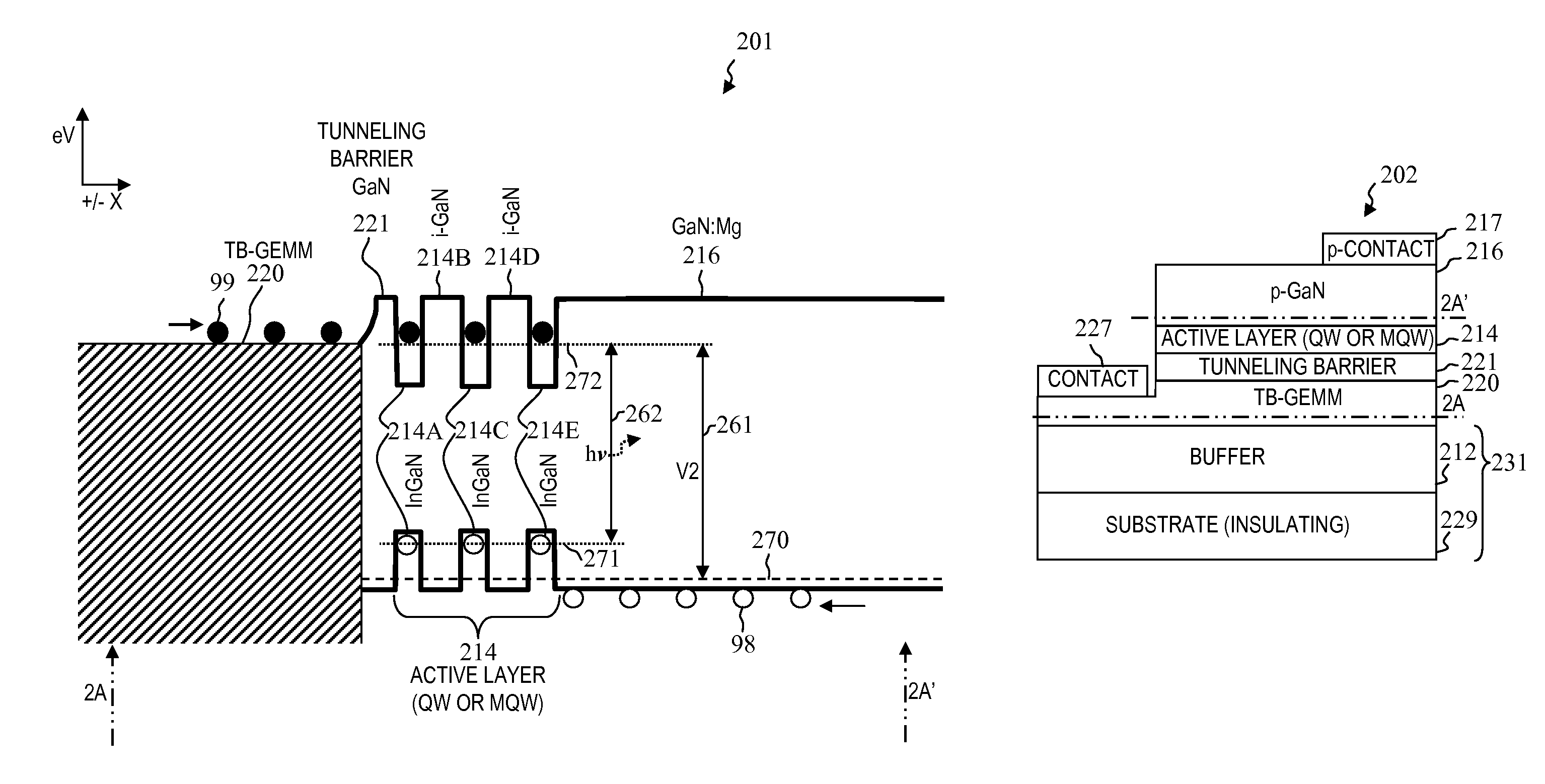
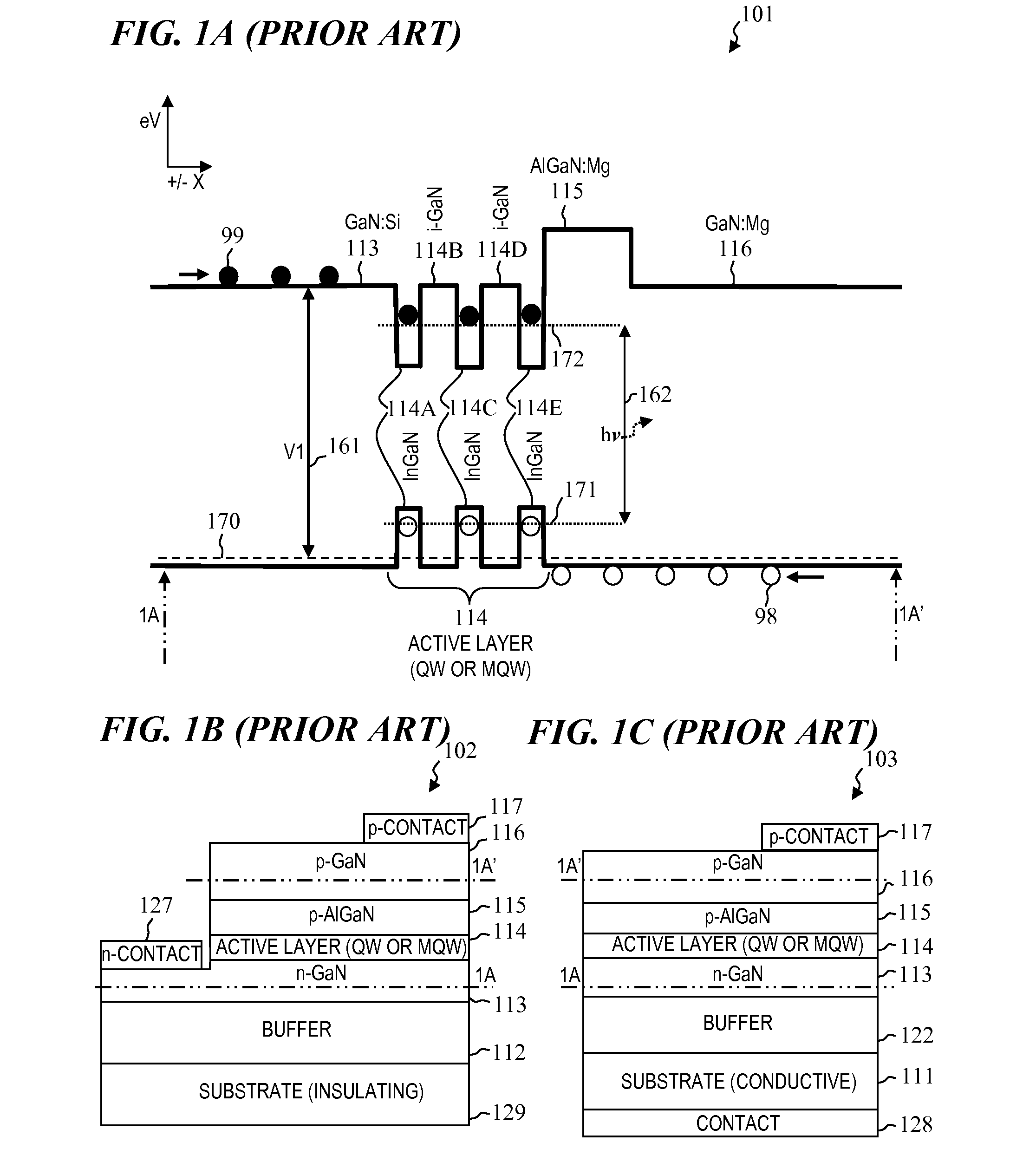
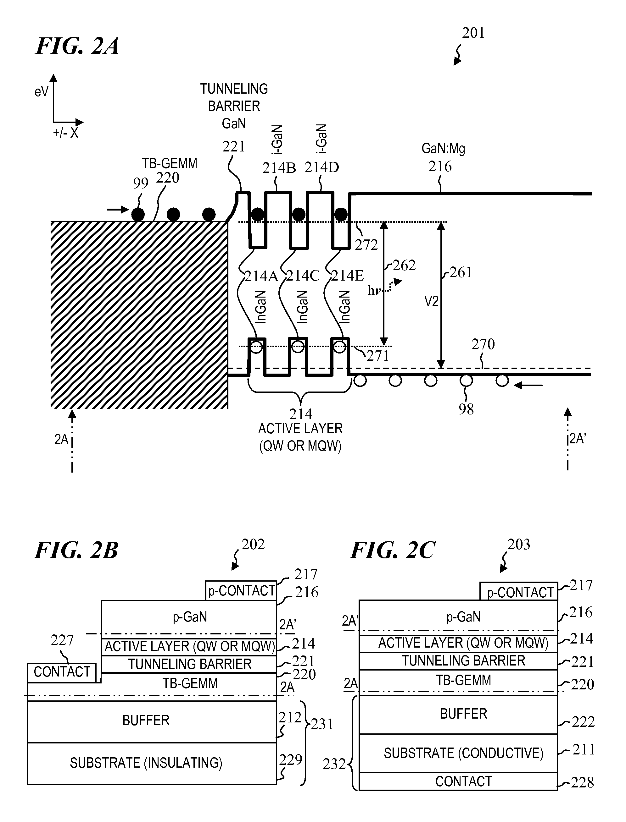
[0053]In the following detailed description of the preferred embodiments, reference is made to the accompanying drawings that form a part hereof, and in which are shown by way of illustration specific embodiments in which the invention may be practiced. It is understood that other embodiments may be utilized and structural changes may be made without departing from the scope of the present invention.

[0054]The leading digit(s) of reference numbers appearing in the Figures generally corresponds to the Figure number in which that component is first introduced, such that the same reference number is used throughout to refer to an identical component which appears in multiple Figures. Signals and connections may be referred to by the same reference number or label, and the actual meaning will be clear from its use in the context of the description.

[0055]Device structures including various configurations of an epitaxially grown metal mirror are described. As used herein, these embedded mi...


PUM

PropertyMeasurementUnit
thicknessaaaaaaaaaa
thicknessaaaaaaaaaa
thicknessaaaaaaaaaa

Abstract

An apparatus and method for making it. Some embodiments include a light-emitting device having a light-emitting active region; a tunneling-barrier (TB) structure facing adjacent the active region; a TB grown-epitaxial-metal-mirror (TB-GEMM) structure facing adjacent the TB structure, wherein the TB-GEMM structure includes at least one metal is substantially lattice matched to the active region; and a conductivity-type III-nitride crystal structure adjacent facing the active region opposite the TB structure. In some embodiments, the active region includes an MQW structure. In some embodiments, the TB-GEMM includes an alloy composition such that metal current injectors have a Fermi energy potential substantially equal to the sub-band minimum energy potential of the MQW. Some embodiments further include a second mirror (optionally a GEMM) to form an optical cavity between the second mirror and the TB-GEMM structure. In some embodiments, at least one of the GEMM is deposited on, and lattice matched to, a substrate.

Description

RELATED APPLICATIONS[0001]This application claims benefit under 35 U.S.C. §119(e) of U.S. Provisional Patent Application No. 61 / 066,960, filed Feb. 25, 2008, which is incorporated herein by reference in its entirety.[0002]The application is related to U.S. patent application Ser. No. 11 / 882,730, filed Aug. 3, 2007, titled III-NITRIDE LIGHT-EMITTING DEVICES WITH ONE OR MORE RESONANCE REFLECTORS AND REFLECTIVE ENGINEERED GROWTH TEMPLATES FOR SUCH DEVICES, AND METHODS, which is incorporated herein by reference in its entirety for all purposes.FIELD OF THE INVENTION[0003]The present invention relates to semiconductor light emitters and devices, and more particularly to an apparatus and method of manufacture of group III-nitride light-emitting diodes (LEDs), some embodiments of which provide a vertical-structure LED, and optionally include group III-nitride LEDs, GaN-based LEDs, and semiconductor laser diodes.BACKGROUND OF THE INVENTION[0004]This invention is related to III-Nitride based...

Claims


Application Information

Patent Timeline
Patent Type & Authority Patents(United States)
IPC IPC(8): H01L29/06H01L33/04H01L33/06H01L33/10H01L33/40
CPCH01L33/405H01L33/105H01L33/04H01L33/06Y10T29/5313
Inventor JORGENSON, ROBBIE J.KING, DAVID J.
Owner LIGHTWAVE PHOTONICS INC
Why Eureka
Try Eureka