Millimeter wave monolithic integrated circuits and methods of forming such integrated circuits

a monolithic integrated circuit and integrated circuit technology, applied in the direction of amplifiers with semiconductor devices/discharge tubes, amplifiers with min 3 electrodes or 2 pn junctions, amplifiers with semiconductor devices only, etc., can solve the problems of high frequency, millimeter wave integrated circuit devices that are difficult to manufacture, and do not function similarly or adequately. , the effect of reducing the number of transistors

Active Publication Date: 2010-11-30
RAYTHEON CO
View PDF9 Cites 4 Cited by
  • Summary
  • Abstract
  • Description
  • Claims
  • Application Information

AI Technical Summary

Problems solved by technology

The design and manufacture of high frequency, millimeter wave integrated circuit devices presents many challenges not found in the construction of other types of integrated circuits.
However, the design and manufacture of circuits for operation in the W-band and above, frequencies of approximately 75 GHz and above, present particular challenges, as circuits and structures suitable for use even at lower millimeter wave frequencies, for example as may be suitable for devices operating at 30 GHz, do not function similarly or adequately at 75 GHz and above.
Additionally, however, the placement and configuration of signal and voltage lines can present substantial problems of resonance or “ringing” of the circuits.
These problems are heightened when the integrated circuit is an amplifier, particularly one offering relatively high gain and power; and particularly when there is a need to form the amplifier in a minimal area on a substrate, for example a minimally-sized semiconductor die.
While these design rules are generally effective for such purposes, the resulting large spaces increase the total area occupied on a die by such an amplifier.
Such a structure, and the routing of voltage lines from the peripheral busses to individual amplifier stages, with the lines surrounded by substantial open area to reduce the risk of interference that result from such a structure, again require additional space on a die, and thereby again increase the relative size of the die.
Accordingly, for such high frequency millimeter wave amplifiers, the conventional design criteria and methodology tend to increase the size of the device where compactness would be an asset.

Method used


Image

  • Millimeter wave monolithic integrated circuits and methods of forming such integrated circuits
  • Millimeter wave monolithic integrated circuits and methods of forming such integrated circuits
  • Millimeter wave monolithic integrated circuits and methods of forming such integrated circuits

Examples


Embodiment Construction

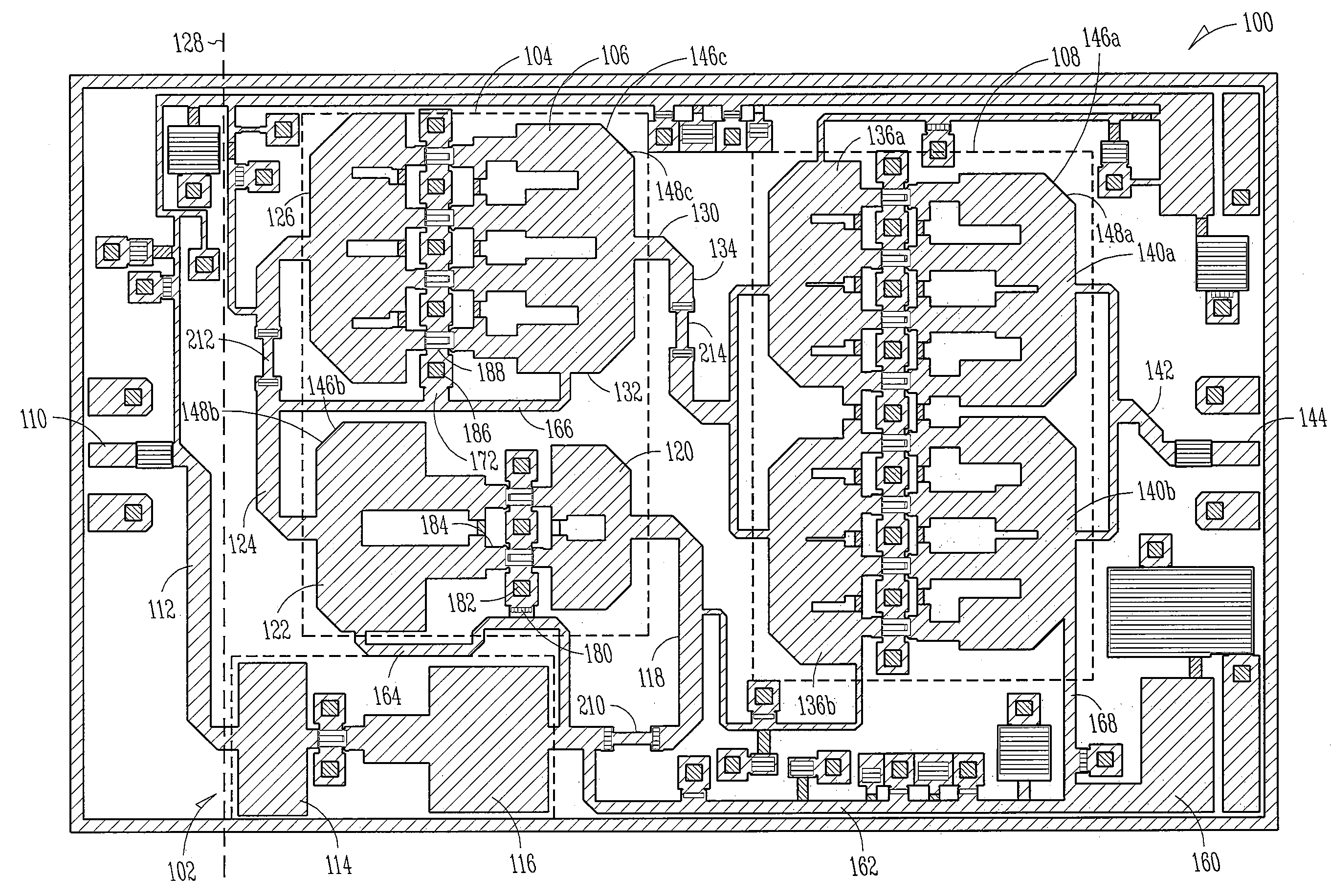
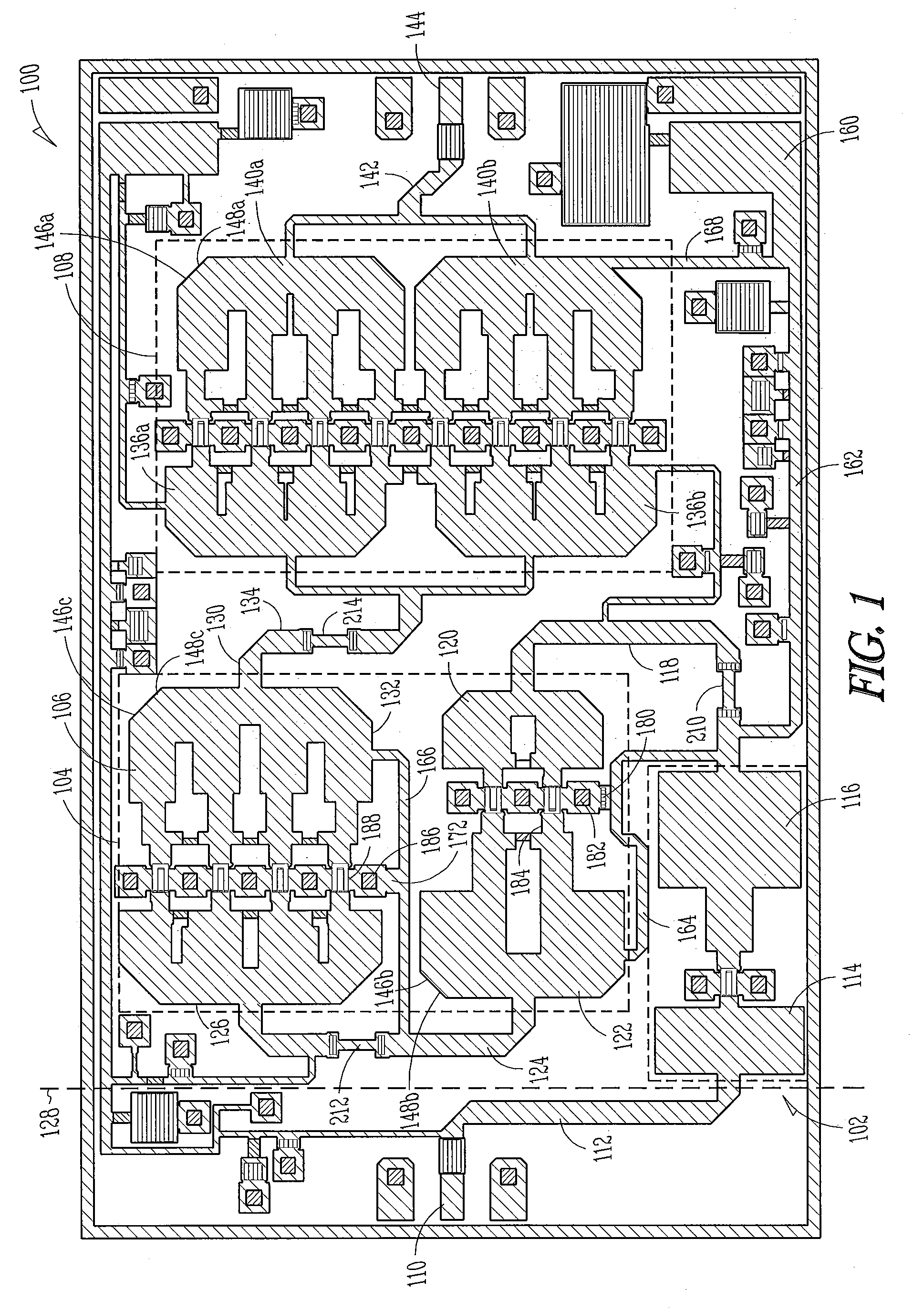
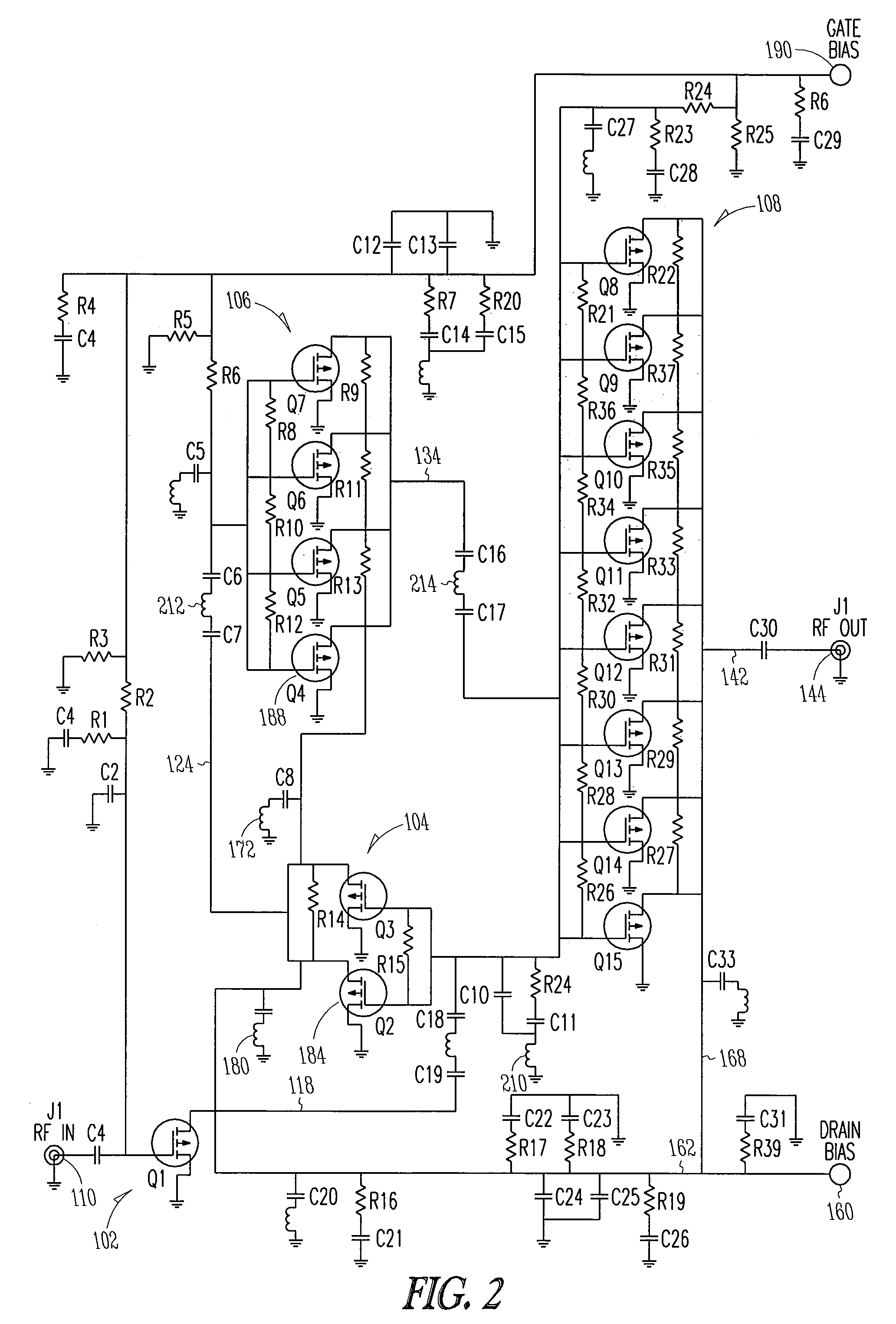
[0013]Referring now to the drawings in more detail, and particularly to FIG. 1, the figure depicts an example layout for a multi-staged, millimeter wave amplifier integrated circuit 100, illustrating various aspects of the present inventive subject matter. As noted earlier herein, the present invention is specifically directed to a multi-stage, millimeter wave amplifier's operating act 75 GHz and above. Additionally, for the present inventors, configuration of amplifiers operating at 90 GHz and above has been a particular concern; and example amplifier 100 is intended for operation at 95 GHz. For purposes of the present disclosure, relatively high gain amplifiers, as can particularly benefit from the principles described herein, are considered those operating at a frequency at or above 75 GHz, and providing at least 15 db of gain, and a power of a least 1 Watt. In accordance with the principles described herein, and amplifier meeting at least two or more of these performance objecti...


PUM


Abstract

A description is provided of a high-frequency, multi-stage, millimeter wave amplifier integrated circuit, and of a method for designing and constructing the circuit. The methods and structures have been created to enable the construction of an amplifier offering substantial gain at a relatively high power and high frequency, but occupying minimal area of an integrated circuit die. Various structures and methodologies are described which each contribute to the practical feasibility of constructing an amplifier with such performance in a relatively compact space.

Description

BACKGROUND OF THE INVENTION[0001]The present invention relates generally to high frequency millimeter wave integrated circuit amplifiers, and more particularly relates to such high frequency amplifiers configured for use at frequencies of 75 GHz and higher.[0002]The design and manufacture of high frequency, millimeter wave integrated circuit devices presents many challenges not found in the construction of other types of integrated circuits. However, the design and manufacture of circuits for operation in the W-band and above, frequencies of approximately 75 GHz and above, present particular challenges, as circuits and structures suitable for use even at lower millimeter wave frequencies, for example as may be suitable for devices operating at 30 GHz, do not function similarly or adequately at 75 GHz and above.[0003]As will be apparent to those skilled in the art, structures such as filters suitable for use at the identified higher frequencies must be adapted for such frequencies. A...

Claims


Application Information

Patent Timeline
Patent Type & Authority Patents(United States)
IPC IPC(8): H03F3/14
CPCH03F3/195H03F3/211
Inventor BROWN, KENNETH W.BROWN, ANDREW K.
Owner RAYTHEON CO
Why Eureka
Try Eureka