Method of producing pattern-formed structure and photomask used in the same
a technology of pattern-forming structure and photomask, which is applied in the direction of photo-taking process, photomechanical apparatus, instruments, etc., can solve the problems of high-precision pattern formation, product deterioration, and waste liquid must be properly treated before discarding, so as to achieve excellent modification efficiency and high quality.
- Summary
- Abstract
- Description
- Claims
- Application Information
AI Technical Summary
Benefits of technology
Problems solved by technology
Method used
Image
Examples
example 1
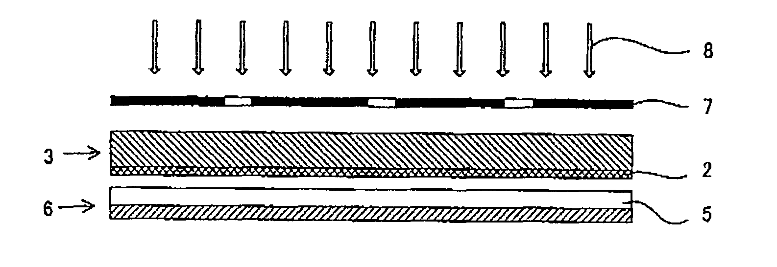
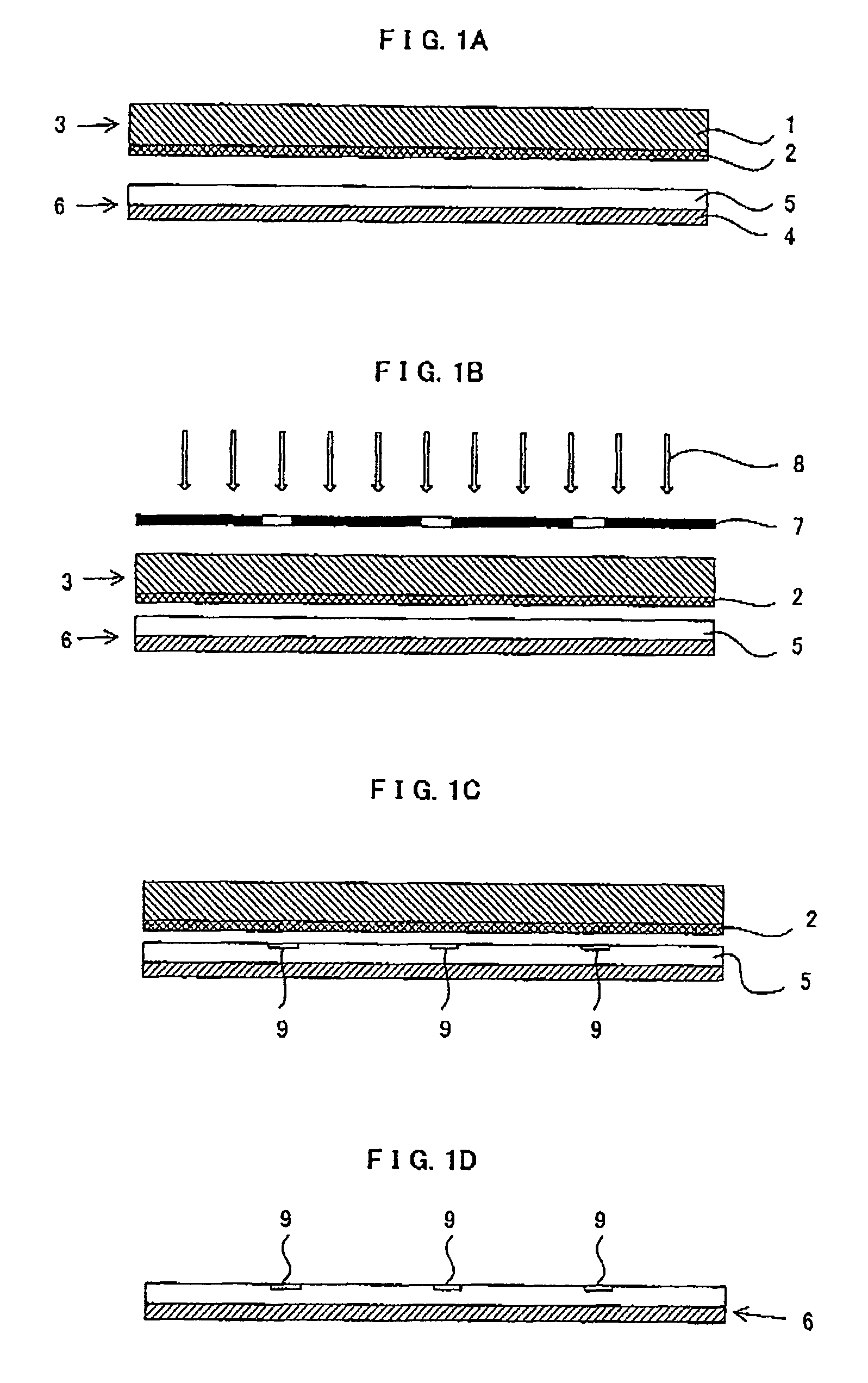
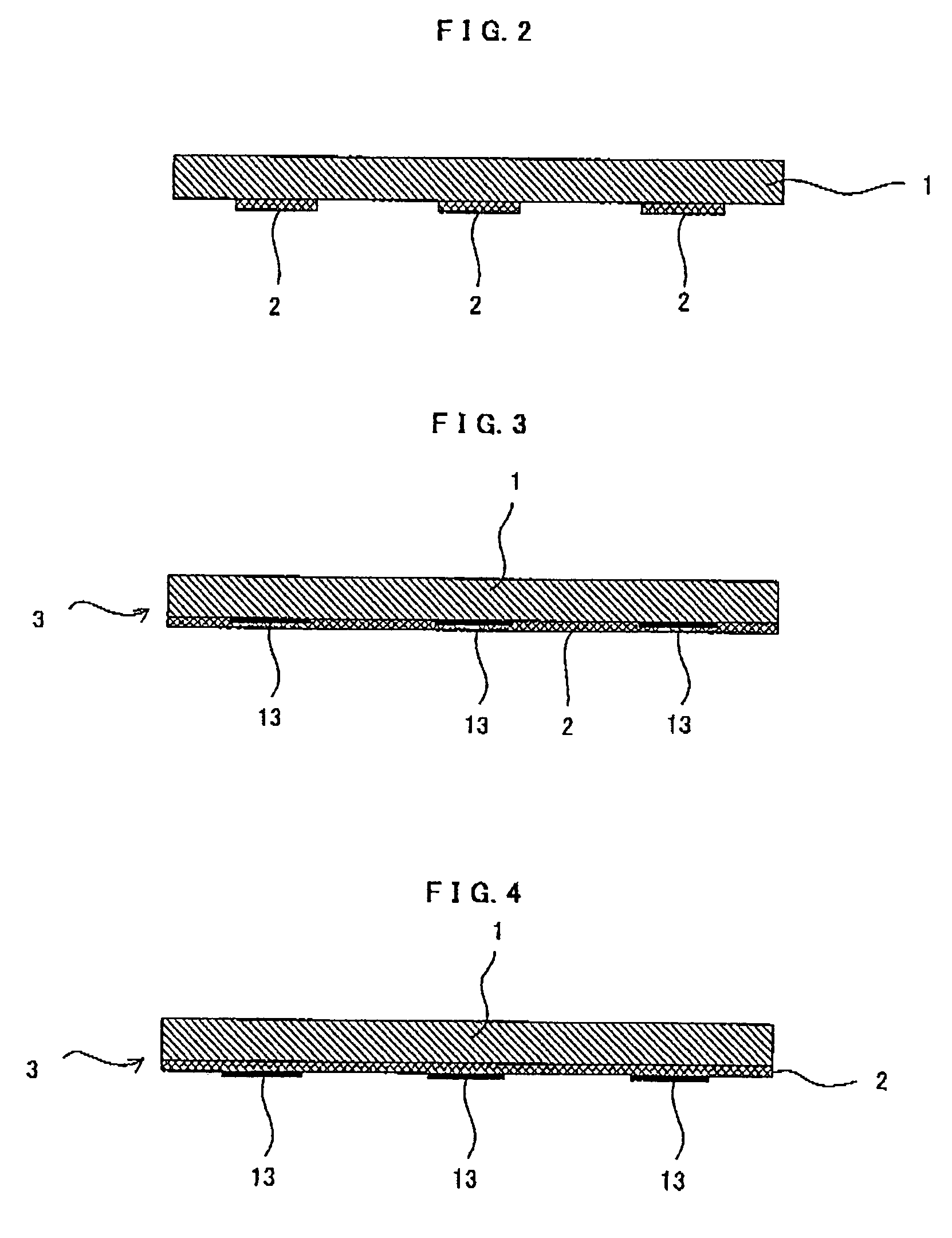
[0252]On a quartz glass substrate including a pattern as a chrome-made light-shielding portion, of 0.4 μm thickness and 100 μm line-and-space, formed on the substrate, a titanium oxide coating agent for photocatalyst (TKC301, manufactured by TEIKA Co., Ltd.) was applied by coating. The substrate was dried at 350° C. for 3 hours, whereby a photomask including a photocatalyst-containing layer (the photocatalyst-containing-layer side substrate) was obtained.
[0253]Next, 3 g of 0.1 N hydrochloric acid (aq) was added to 5 g of methyltrimethoxysilane and the mixture was stirred for 1 hour at the room temperature. The resulting solution was applied by coating on a glass substrate. The glass substrate was then dried at 150° C. for 10 minutes, whereby a wetting-property-modifiable layer was formed.
[0254]The photomask and the substrate for a pattern-formed structure obtained as described above were closely attached to each other and ultraviolet was irradiated by an extra-high pressure mercury ...
example 2
[0255]A pattern formation was carried out in the substantially same manner as that of example 1, except that the thickness of the chrome-made pattern-formed structure was 0.1 μm. As a result, it took 370 seconds for the contact angle formed by water at the exposed portion of the wetting-property-modifiable layer to decrease to 10° or smaller.
example 3
[0256]A pattern formation was carried out in the substantially same manner as that of example 1, except that the light-shielding portion pattern of example 1 was replaced with a light-shielding portion pattern having thickness of 20 μm and made of a resin binder in which carbon black had been dispersed. As a result, it took 560 seconds for the contact angle formed by water at the exposed portion of the wetting-property-modifiable layer to decrease to 10° or smaller.
PUM
| Property | Measurement | Unit |
|---|---|---|
| thickness | aaaaa | aaaaa |
| distance | aaaaa | aaaaa |
| contact angle | aaaaa | aaaaa |
Abstract
Description
Claims
Application Information


