Through substrate via process

a technology of through substrate and substrate layer, which is applied in the direction of semiconductor/solid-state device manufacturing, basic electric elements, electric apparatus, etc., can solve the problems of high temperature during the fabrication of the semiconductor device to be formed, affecting the performance of the device, and raising the difficulty of the cmp process

Active Publication Date: 2010-12-07
UNITED MICROELECTRONICS CORP
View PDF3 Cites 41 Cited by
  • Summary
  • Abstract
  • Description
  • Claims
  • Application Information

AI Technical Summary

Benefits of technology

[0010]Accordingly, the present invention is directed to a TSV process, such that the conductive material disposed in the holes can be prevented from damage under high temperature, and the substrate is free of contamination.
[0022]As mentioned above, the TSV process of the present invention is carried out by filling the holes with the dielectric layer instead of the conductive layer, and then performing the semiconductor process on the substrate, which is followed by removing the dielectric layer from the holes and filling the holes with the conductive layer. Accordingly, the contamination formed on the substrate can be avoided, and the conductive layer can be prevented from damage caused by the high temperature during the semiconductor process.

Problems solved by technology

When the conductive material filling the holes is metal, contamination usually occurs on the wafer which makes a great impact on the subsequent process, and the metal filling the holes cannot endure the high temperature during the fabrication of the semiconductor device to be formed, e.g. the high temperature of conducting a thermal oxidation process for forming a gate dielectric layer, and the high temperature of conducting a source / drain region activation process.
In addition, if the holes are filled with polysilicon to prevent the contamination problem mentioned above, the performance of the device is affected due to high resistance of polysilicon.
Nevertheless, after the holes are filled with the conductive material, difficulty in the CMP process is raised because the semiconductor device has been formed on the substrate.
Besides, complexity of the interconnect process is often raised owing to reservation of the space for TSV process.
However, the bonding material utilized for bonding the wafers is usually damaged due to the incapability to bear the high temperature during the TSV process, so that the wafers cannot be bonded together.

Method used


Image

  • Through substrate via process
  • Through substrate via process
  • Through substrate via process

Examples


Embodiment Construction

[0026]Reference will now be made in detail to the present preferred embodiments of the invention, examples of which are illustrated in the accompanying drawings. Wherever possible, the same reference numbers are used in the drawings and the description to refer to the same or like parts.

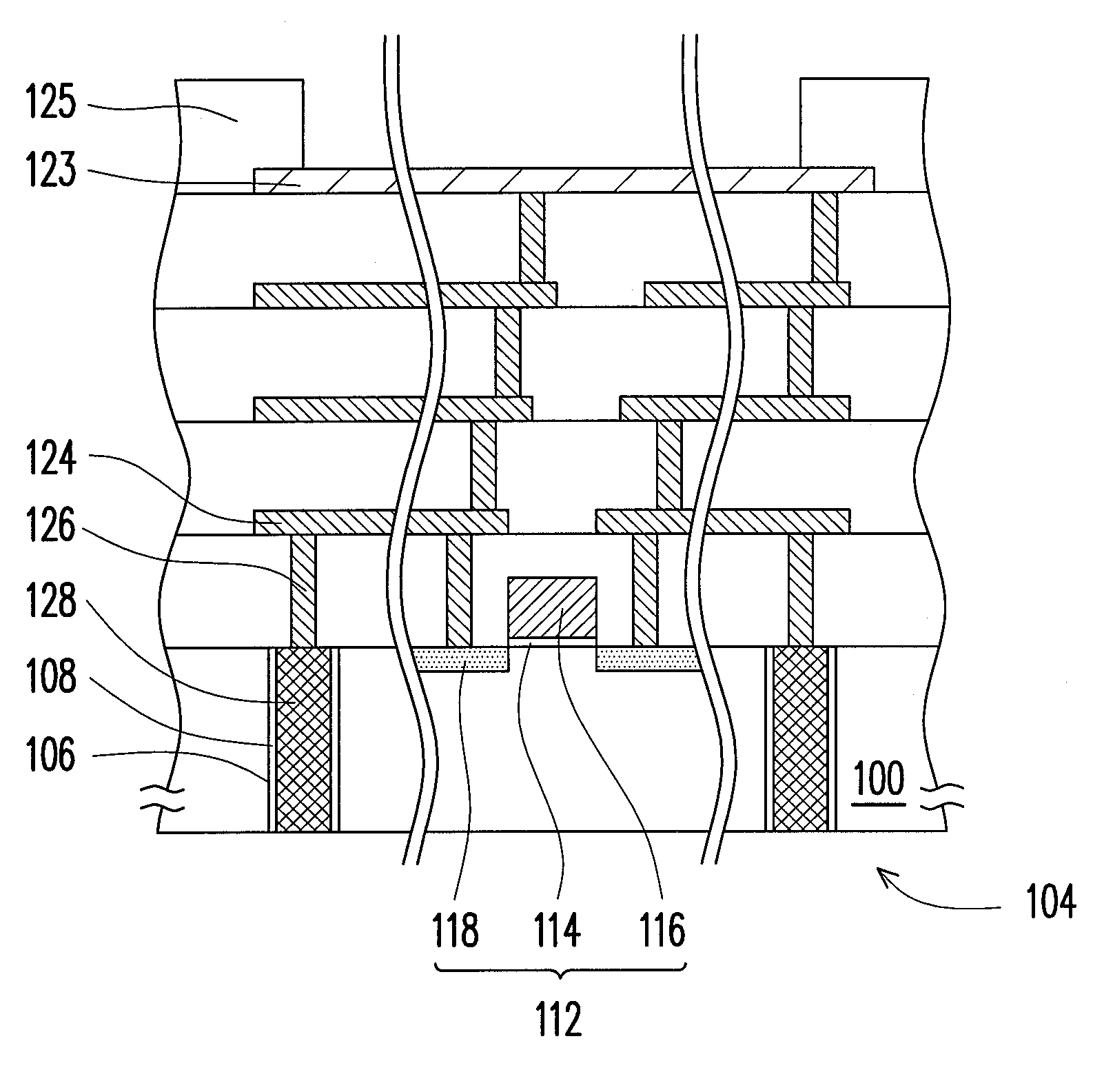
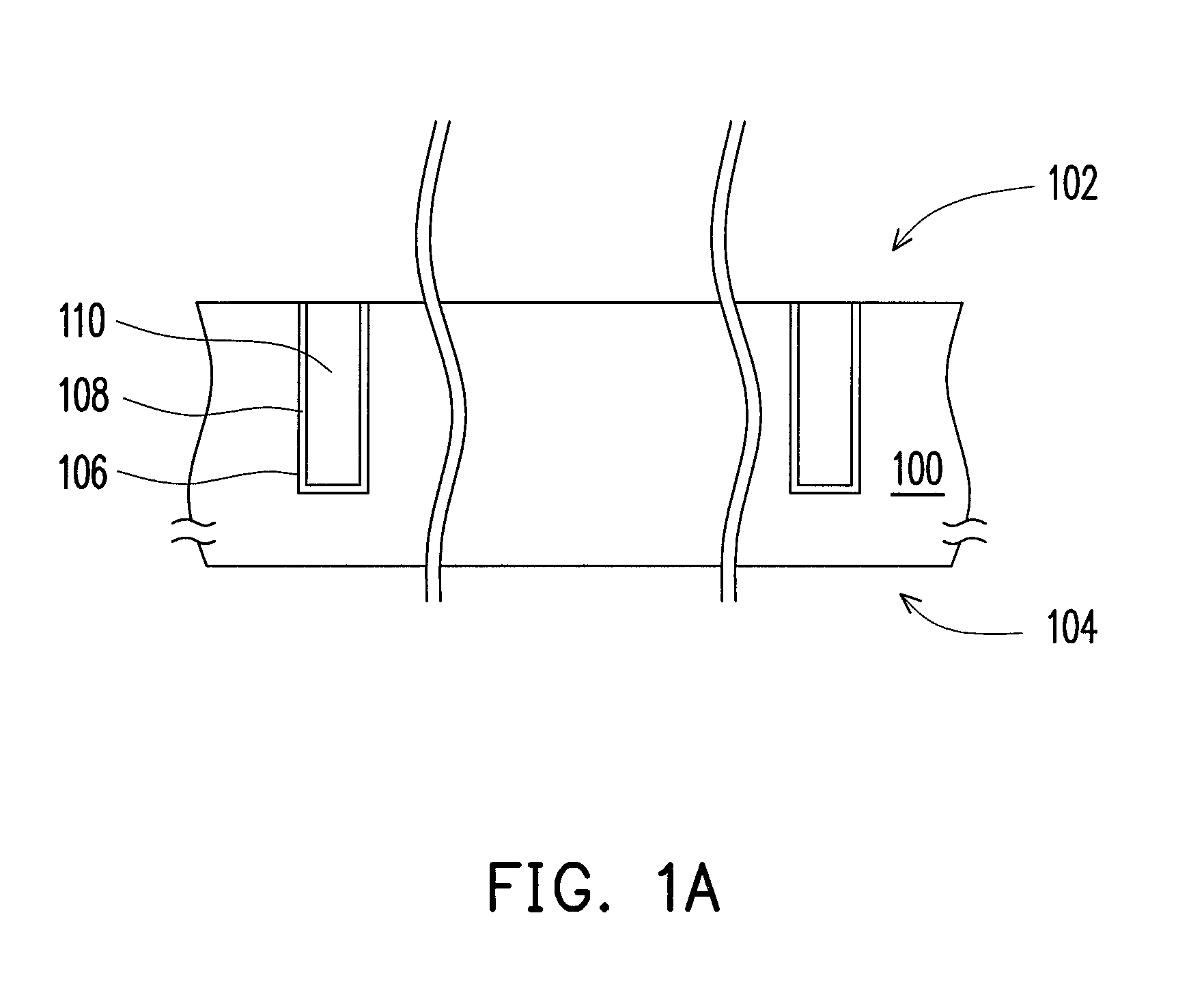
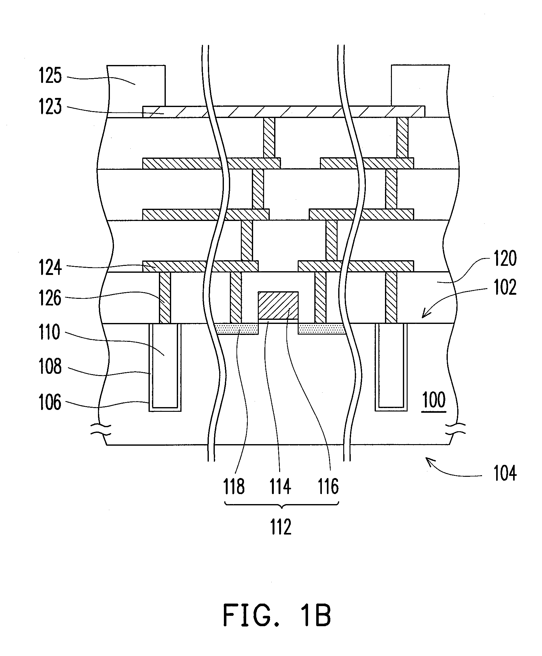
[0027]FIGS. 1A-1D depict, in a cross-sectional view, a TSV process according to an embodiment of the present invention. Referring to FIG. 1A, a substrate 100 is provided, which may be a silicon substrate. The substrate 100 has a first side 102 and a second side 104 opposite to each other. Holes 106 are then formed in the substrate 100 at the first side 102. The method for forming the holes 106 is, for example, performing a lithography process and an etching process in sequence. Subsequently, a dielectric layer 108 is formed on the substrate 100. The material of the dielectric layer 108 may be silicon oxide or silicon nitride, and the forming method thereof can utilize CVD to form the film conformally...


PUM


Abstract

A through substrate via (TSV) process is provided. A substrate having a first side and a second side opposite the first side is provided. A plurality of holes is formed in the substrate at the first side. A first dielectric layer is formed on a sidewall and a bottom of the holes. A second dielectric layer is formed in the holes, wherein a material of the second dielectric layer is different from that of the first dielectric layer. A semiconductor device and an interconnect are formed on the substrate at the first side. At least a portion of the substrate at the second side is removed to expose the second dielectric layer in the holes. The second dielectric layer is removed. A conductive layer is formed in the holes.

Description

BACKGROUND OF THE INVENTION[0001]1. Field of the Invention[0002]The present invention generally relates to a semiconductor process, and in particular, to a through substrate via (TSV) process.[0003]2. Description of Related Art[0004]Along with the rapid development in techniques of the semiconductor process, further improvement in integration and performance of the semiconductor device is demanded, which advances the development in the structure of stacking wafers. The TSV process is one of the common techniques for fabricating the stacked wafer structure. During the TSV process, holes with high aspect ratio are first formed in the substrate of the wafer, and are then filled with a conductive material. Subsequently, a chemical mechanical polishing (CMP) process is performed, so as to remove the conductive material disposed outside the holes. Afterwards, a portion of the substrate at the backside is removed, so as to thin the substrate and expose the conductive material disposed in t...

Claims


Application Information

Patent Timeline
Patent Type & Authority Patents(United States)
IPC IPC(8): H01L21/44
CPCH01L21/76898
Inventor KUO, CHIEN-LI
Owner UNITED MICROELECTRONICS CORP
Why Eureka
Try Eureka