Semiconductor device having solder-free gold bump contacts for stability in repeated temperature cycles

a technology of solder-free gold bumps and semiconductor devices, which is applied in the manufacture of printed circuits, printed circuit aspects, basic electric elements, etc., can solve the problems of poor performance of solder-attached gold bumps and rapid increase of electrical resistance of gold-solder contacts, and achieve the effect of increasing contact resistan

Active Publication Date: 2010-12-07
TEXAS INSTR INC
View PDF11 Cites 65 Cited by
  • Summary
  • Abstract
  • Description
  • Claims
  • Application Information

AI Technical Summary

Problems solved by technology

It has been found routinely that solder-attached gold bumps fare poorly in these temperature excursions; the electrical resistance of the gold-solder contacts increases rapidly, or the gold bump dissolves in the molten solder alloy, or the contacts open altogether after only three or four temperature cycles.

Method used


Image

  • Semiconductor device having solder-free gold bump contacts for stability in repeated temperature cycles
  • Semiconductor device having solder-free gold bump contacts for stability in repeated temperature cycles
  • Semiconductor device having solder-free gold bump contacts for stability in repeated temperature cycles

Examples


Embodiment Construction

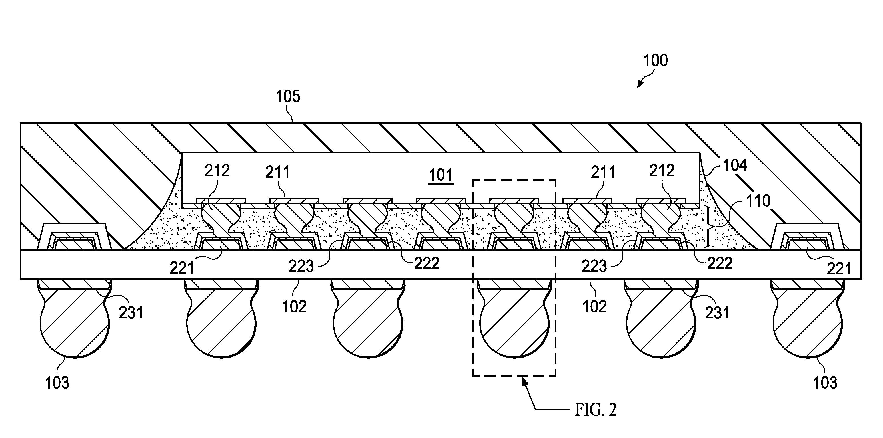
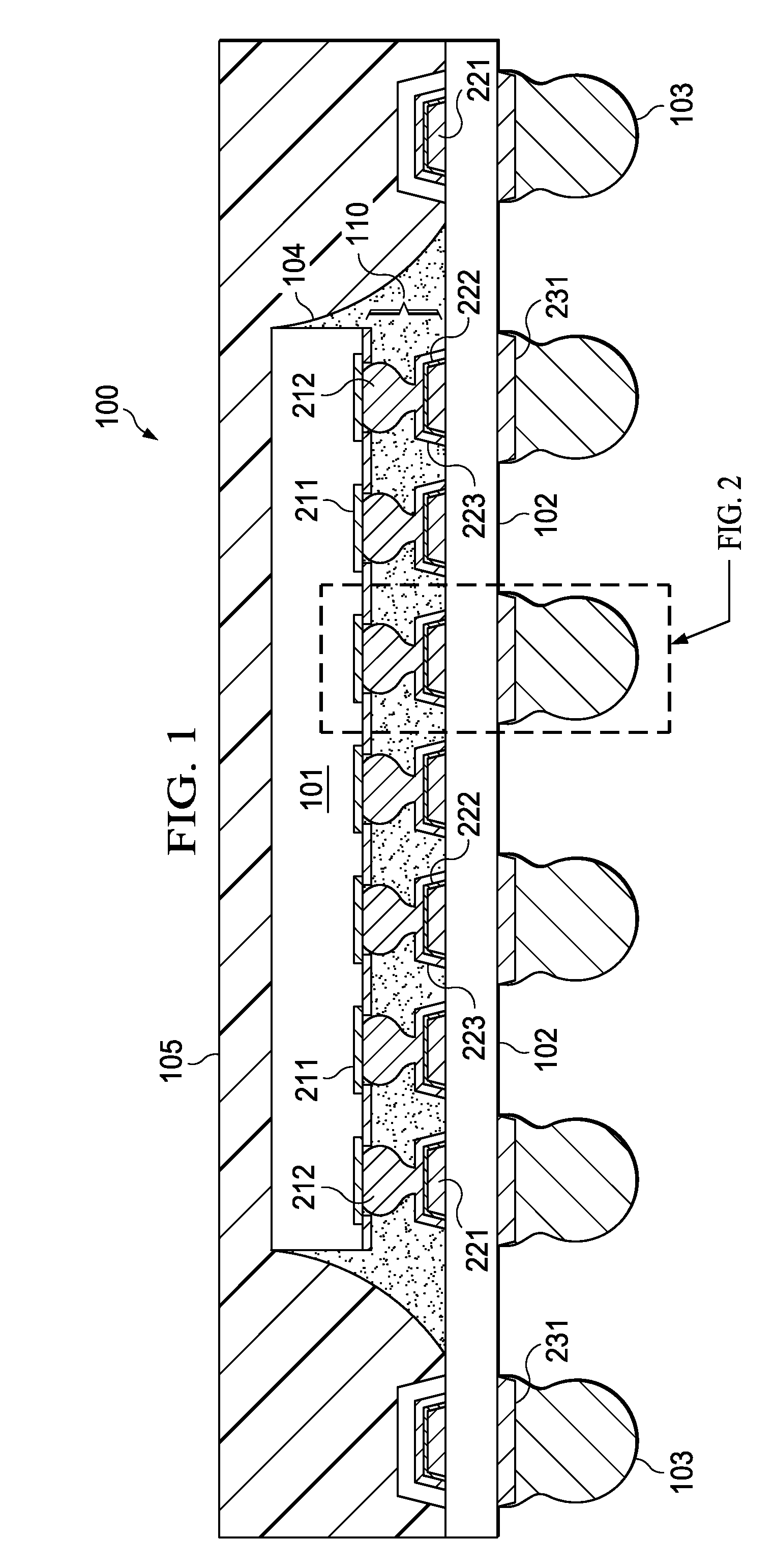
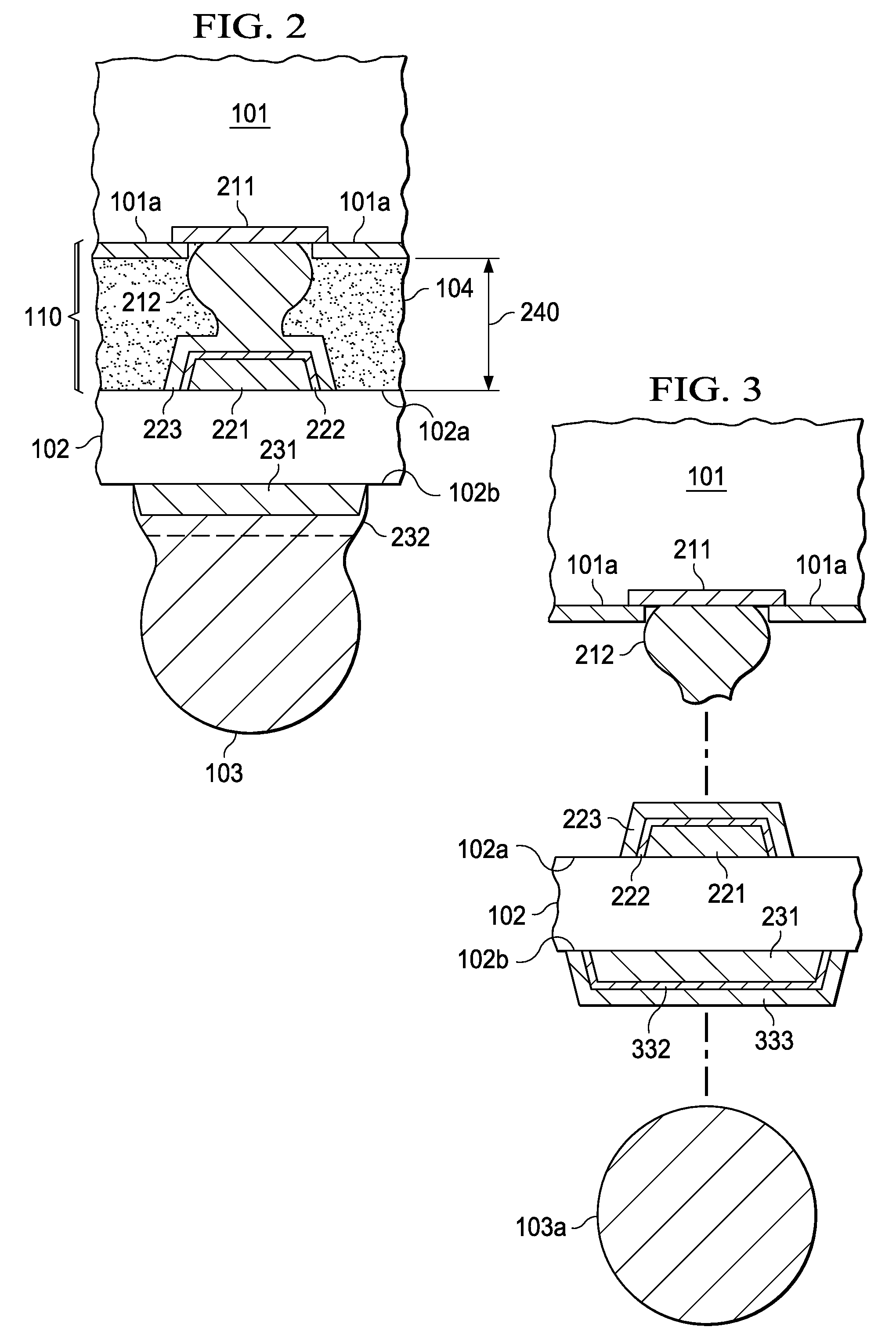
[0014]An embodiment of the invention is a metallic interconnect structure 110 for connecting a gold stud to a copper contact pad without the use of solder. FIG. 1 illustrates a packaged semiconductor device, generally designated 100, which includes a plurality of interconnect structures 110. A semiconductor chip 101 is assembled on a substrate 102 using these interconnect structures. Device 100 of FIG. 1 has a single chip 101; in other embodiments, there may be more than one chip, or one or more stacks of chips. Attached to the substrate on the surface opposite to the chip are reflow bodies 103, which are suitable for connection to external parts. Device 100 further includes a polymeric precursor 104, which fills the spaces between the interconnect structures, and an encapsulation compound 105 for protecting the assembled chip. In some embodiments, precursor 104 is not needed, because it is replaced by compound 105; in still other embodiments, compound 105 is not needed.

[0015]A port...


PUM

PropertyMeasurementUnit
thicknessaaaaaaaaaa
thicknessaaaaaaaaaa
thicknessaaaaaaaaaa

Abstract

A semiconductor device has a chip (101) with gold studs (212) assembled on a tape substrate (102), which has solder balls (103) for attachment to external parts. The tape substrate (about 30 to 70 μm thick) has on its first surface first copper contact pads (221) covered with a continuous thin nickel layer (222) of about 0.04 to 0.12 μm thickness. Gold including stud (212) is contacting the nickel. On the second substrate surface are second copper contact pads (231) covered with an alloy layer (about 2 to 3 μm thick) including gold, copper / tin alloys, and copper / nickel / tin alloys; the alloys are metallurgically attached to the second copper pad and substantially free of unalloyed nickel. A reflow body (103) comprising tin is metallurgically attached to the alloy layer of each second pad.

Description

FIELD OF THE INVENTION[0001]The present invention is related in general to the field of semiconductor devices and processes, and more specifically to metallurgical systems for stable gold bump connections with and without solder.DESCRIPTION OF RELATED ART[0002]The growing popularity of flip-chip assembly in the fabrication process flow of silicon integrated circuit (IC) devices is driven by several facts. First, the electrical performance of the semiconductor devices can be improved when the parasitic inductances correlated with conventional wire bonding interconnection techniques are reduced. Second, flip-chip assembly provides higher interconnection densities between chip and package than wire bonding. Third, flip-chip assembly consumes less silicon “real estate” than wire bonding, and thus helps to conserve silicon area and reduce device cost. And fourth, the fabrication cost can be reduced, when concurrent gang-bonding techniques are employed rather than consecutive individual b...

Claims


Application Information

Patent Timeline
Patent Type & Authority Patents(United States)
IPC IPC(8): H01L23/48H01L23/52
CPCH01L23/3128H01L23/49811H01L23/49816H01L24/11H01L24/12H01L24/16H01L24/81H05K3/328H05K3/3463H01L23/145H01L2224/0401H01L2224/05624H01L2224/1134H01L2224/1184H01L2224/13144H01L2224/13147H01L2224/16225H01L2224/32507H01L2224/45015H01L2224/81205H01L2224/81801H01L2224/8383H01L2224/85205H01L2924/01004H01L2924/01012H01L2924/01013H01L2924/0102H01L2924/01029H01L2924/01046H01L2924/01047H01L2924/01061H01L2924/01074H01L2924/01079H01L2924/01082H01L2924/01327H01L2924/14H01L2924/20105H01L2924/20106H01L2924/20107H01L2924/20751H01L2924/20752H01L2924/20753H01L2924/30107H05K1/189H05K3/244H05K2201/10674H05K2203/0285H01L2924/00014H01L2224/0558H01L2924/00013H01L2924/01005H01L2924/01006H01L2924/01033H01L2924/0105H01L2924/014H01L2224/13099H01L2224/45147H01L2924/00H01L2224/48624H01L2924/01014H01L2924/01028H01L2224/32225H01L2224/73204H01L2224/45144H01L2924/10253H01L2224/48824H01L2924/00011H01L2224/83205
Inventor MASUMOTO, MUTSUMI
Owner TEXAS INSTR INC
Why Eureka
Try Eureka