Semiconductor device

a semiconductor device and semiconductor technology, applied in the direction of generating/distributing signals, instruments, sustainable buildings, etc., can solve the problems of voltage temporarily decreasing, noise generation in the power source, and the reduction of power consumption of the semiconductor device becomes a big problem

Inactive Publication Date: 2010-12-07
SOCIONEXT INC
View PDF7 Cites 19 Cited by
  • Summary
  • Abstract
  • Description
  • Claims
  • Application Information

AI Technical Summary

Problems solved by technology

In recent years, as semiconductor devices (semiconductor integrated circuits) such as large-scale integrations (LSIs) are increased in speeds and sizes, reduction of power consumption in the semiconductor devices becomes a big problem.
However, to the particular block, if the power supply on / off control, the changing control of the operating voltages, the changing control of the operating frequencies, and the on / off control relating to the operating frequency are performed, noise can be generated in the power source or a ground in the semiconductor device, or the voltage can be temporarily decreased (for example, see FIG. 13).
Further, in a normal operation where the operating voltage and the operating frequency are constant, due to simultaneous switching output noise (SSO noise) in changing outputs such as input / output (I / O) cells (input / output circuits) at once or the like, noise can be generated in the power source or the ground in the semiconductor device.
The power-supply noise or the temporary voltage reduction in the semiconductor device can affect the operation of the semiconductor device and may cause malfunction.
Especially, in the semiconductor devices that have the chip divided into power source blocks, capacity of each power source block is small.
Accordingly, the semiconductor devices are easily affected by the power-supply noise and the temporary voltage reduction.
For example, the malfunction in the semiconductor devices caused by large-amplitude noise in the power source or the ground or temporary voltage reduction includes destruction of data stored in a register or a memory, and timing error generation.
Further, a phase locked loop (PLL) may be unlocked and supply clocks may transiently become unexpectedly high frequencies.
Then, the semiconductor devices become unstable and can cause malfunction.
Then, if data is being transferred between the CPU and the on-chip bus, a timing error may be generated and may cause malfunction.
However, in monitoring the operation state using the ring oscillator, if a predetermined period for measuring a count value using the ring oscillator has not passed, it is not possible to determine the operation state of the semiconductor device.
Accordingly, for example, it is difficult to immediately correspond to the change in the operation state due to a sudden operation deterioration factor such as power-supply noise, temporary voltage reduction, or the like.

Method used


Image

  • Semiconductor device
  • Semiconductor device
  • Semiconductor device

Examples


first embodiment

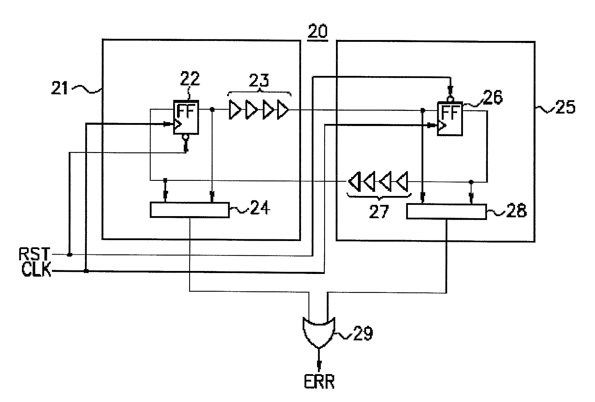
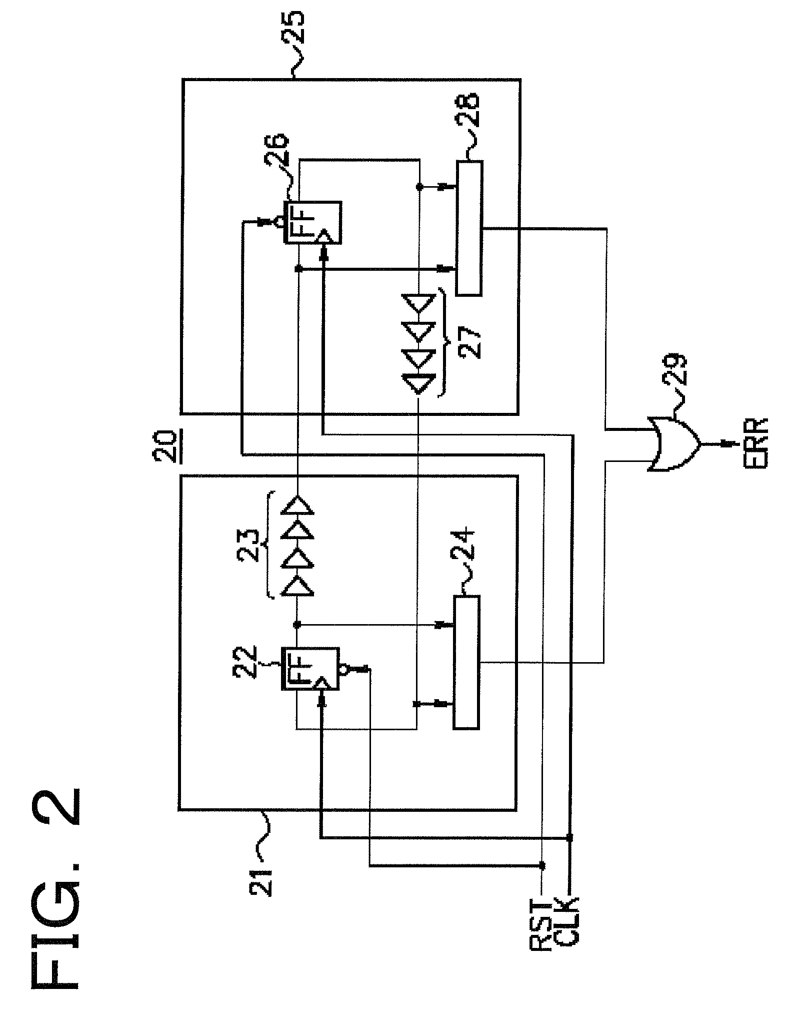
[0033]Hereinafter, a first embodiment will be described.

[0034]As described above, in a case where the circuit for monitoring an operation state in the semiconductor device is realized using the ring oscillator or the like, it is possible to monitor a state averaged to some degree. However, it is difficult to detect malfunction due to an unexpected factor such as an instantaneous power-supply noise, voltage reduction, or the like, or occurrence of a situation that can cause the malfunction. Further, in a case where the detection circuit is formed using analog circuits to detect power-supply noise or the like, it is preferable that stable power-supply voltage without noise is supplied to the detection circuit. However, sometimes it may be difficult to provide the stable power-supply voltage because of limitations in layout or the like.

[0035]The semiconductor device according to the first embodiment is formed using only digital circuits. In the semiconductor device, a malfunction detec...

second embodiment

[0064]Now, a second embodiment is described.

[0065]A semiconductor device according to the second embodiment performs a control to prevent occurrence of a situation that can cause malfunction in a case where the situation that can cause malfunction is detected using the malfunction detection circuit according to the above-described first embodiment. Hereinafter, it is described is an example that in the case where the situation that can cause malfunction is detected, a control is performed such that asynchronous data transfer is performed.

[0066]Generally, when data transfer via a bus is performed between power source blocks that have different operating voltages, the data transfer is performed via an asynchronous bus bridge, or the like. On the other hand, when the data transfer via a bus is performed between power source blocks that have the same operating voltages, the data transfer is performed without using the asynchronous bus bridge, or the like. In such a case, if the operatin...

third embodiment

[0077]Now, a third embodiment is described.

[0078]In a semiconductor device according to the third embodiment, if a situation that can cause malfunction is detected in the above-described semiconductor device according to the second embodiment, further, in a period the operation can become unstable due to the occurrence of the situation that can cause malfunction, the semiconductor device is controlled to reduce an operating frequency in a block that operates at a high speed. In the operation, malfunction such as a timing error due to factors such as instantaneous power-supply noise, voltage reduction, or the like can be prevented.

[0079]FIG. 5 is a view illustrating an example of a configuration of the semiconductor device according to the third embodiment. In FIG. 5, the same reference numerals are applied to structural elements that have the same functions as those illustrated in FIG. 2 or FIG. 4, and overlapped descriptions are omitted.

[0080]In FIG. 5, a clock generation circuit 6...


PUM


Abstract

A semiconductor device includes first and second memory circuits that are disposed in different power source blocks and operate in synchronization with a clock, first and second delay circuits that are connected between output terminals of one memory circuits and input terminals of the other memory circuits, and a determination circuit that determines whether it is a situation that can cause malfunction based on an input signal and an output signal in the memory circuits and outputs a determination result as an error detection signal. To the first and second memory circuits, different initial values are given, and it is monitored whether a signal is sent and received between the memory circuits in a toggle state or not. Thus, occurrence of a situation that can cause malfunction can be simply and quickly detected.

Description

TECHNICAL FIELD[0001]This is related to a semiconductor device that has a plurality of power source blocks in which operating voltages and operating frequencies can be controlled.BACKGROUND[0002]In recent years, as semiconductor devices (semiconductor integrated circuits) such as large-scale integrations (LSIs) are increased in speeds and sizes, reduction of power consumption in the semiconductor devices becomes a big problem. In the semiconductor devices, if a load capacity is C, a power supply voltage is V, and an operating frequency is F, generally, a power consumption P of the semiconductor devices is expressed as P=C×V2×F.[0003]In view of the above, techniques for reducing power consumption of semiconductor devices have been applied to high-speed processors and various semiconductor devices are required to reduce their power consumption to low. The techniques are performed by dividing a chip into a plurality of power source blocks and controlling operating voltages and operatin...

Claims


Application Information

Patent Timeline
Patent Type & Authority Patents(United States)
IPC IPC(8): G11C5/14
CPCG11C29/021G11C5/143H03L7/06G11C29/02G06F1/3203G06F1/08G06F1/3287Y02B60/1278G11C2029/0409Y02B60/1282Y02D10/00
Inventor SHIKATA, TAKASHI
Owner SOCIONEXT INC
Why Eureka
Try Eureka